Forewarning: Bit of a plug for PCBWay in here, but they deserve it. They’re a rad company, and I always like working with them.
Premise:
This project is a reasonably straightforward keyboard / Bluetooth project, that touches a few neat features, without getting too into the weeds. Really the idea is to do a simple product, really well.
I quite like keyboards and some of the associated projects and designs, but have very carefully avoided becoming a keyboard enthusiast. That’s a deep rabbit hole I do not need to go down.
The keyboard community has a really defined keyboard schematic layout, and a really well defined set of variations of features that people may want in a keyboard, and even a particular microcontroller and firmware that they recommend. The firmware, QMK (and ZMK, and maybe some spin-offs) is fully featured, well adopted, and very customisable. From an engineering perspective, it would be irresponsible of me to use anything else.
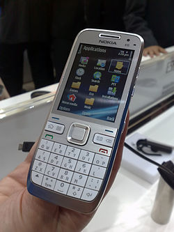
Unless I drastically altered the form factor. So this is a Bluetooth T9/ABC Multitap keyboard based around the keypad of a Nokia E52, as an input device to a smartphone or laptop. For my particular generation only, this typing style is muscle memory. for any other generation, it’s incomprehensible.
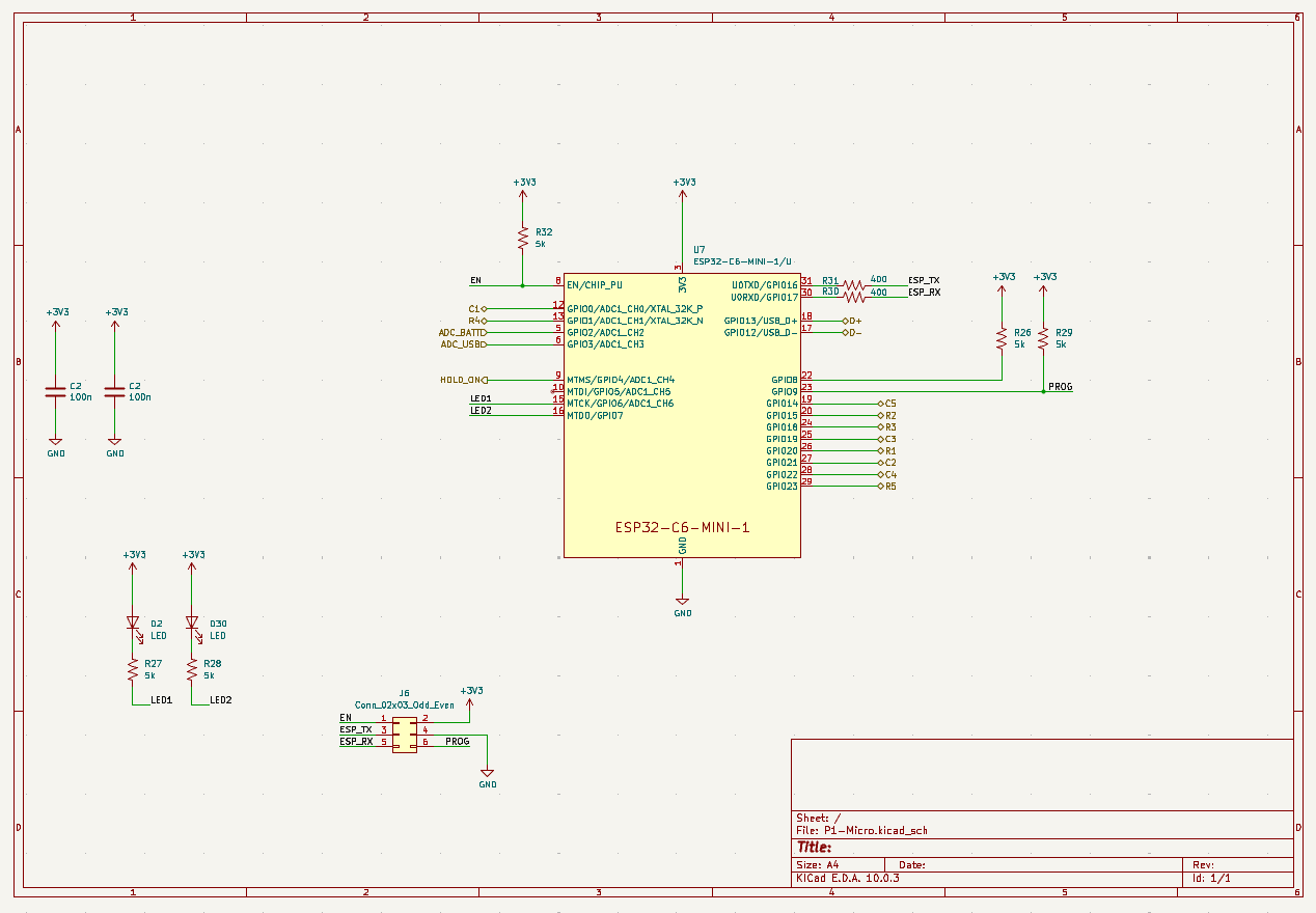
Schematic:
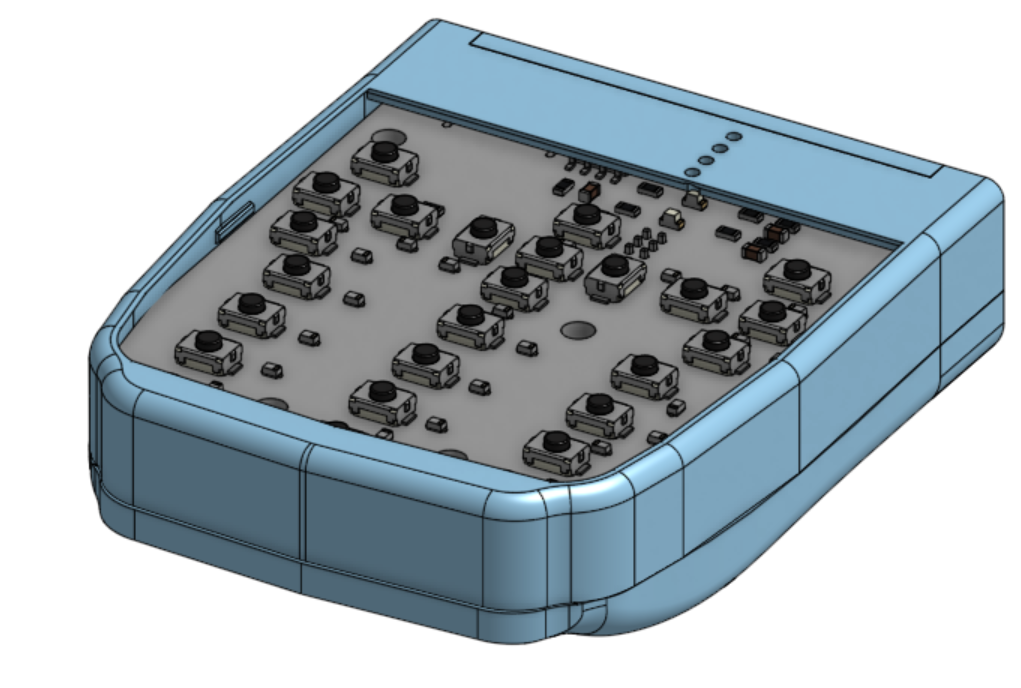
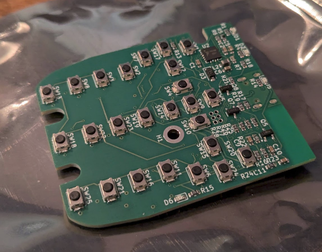
Classic keyboard circuit.
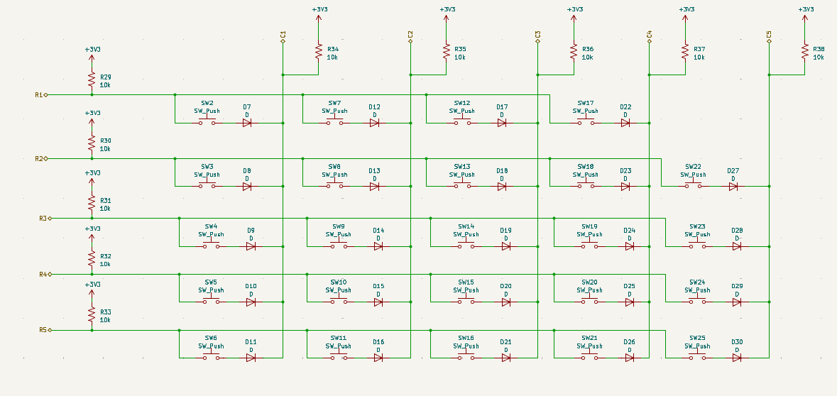
For the keys themselves, I used the Alps SKRK series switches at 0.98N of actuation force. This ends up feeling a little mushy, and I should have gone for the 1.57N version instead. Next time.
I’ve covered battery circuits here before. There are few open source designs out there with proper undervoltage / overcurrent lockout and a proper power path. Where I’ve done this professionally, I’ve used TI’s BQ-series battery management family, which has nice features for a commensurate added cost.
For this one, I played around with a set of classic cheap parts that are sold here by the millions but remain mostly unknown to the western world: the TP4200 battery charger, the DW01A low-voltage / overcurrent cutoff, and a matching 8205A MOSFET pair to disconnect the battery. This is likely the exact combination of parts hiding inside many cheap gadgets you’ll find online, in part because it’s about 25 cents of total BOM cost.
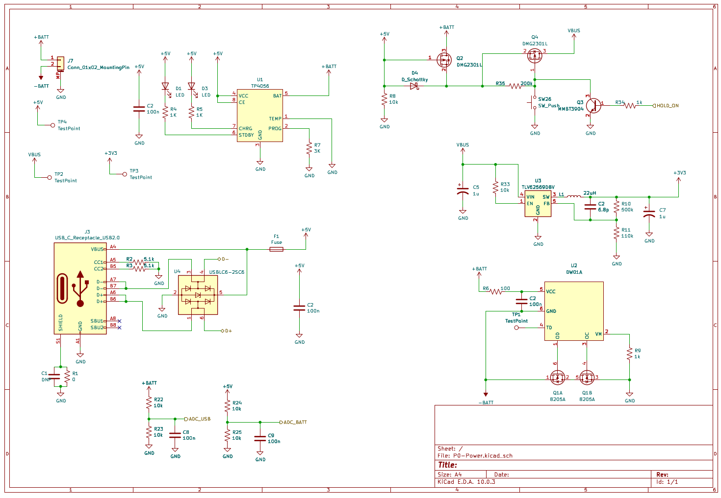
The protection circuit isn’t strictly necessary for this device – the LiPo I used has a protection circuit built into the pouch. That isn’t always the case.
I won’t use this exact circuit again. If I picked similar design considerations next time, some off-the-cuff substitutions would be: the TP5100 (a switching charger) instead of the TP4200 (linear), the PT8261 instead of the DW01A, and I’d actually do some comparison shopping on the 8205A.
The DW01A in my circuit didn’t behave correctly. Under nominal conditions, other OC and OD pins (over-current and over-discharge) are HIGH at all times. My circuit never asserts OD HIGH, and OC is LOW when the USB cable is unplugged.
There are three possibilities:
– I’ve read / implemented the schematic wrong. It doesn’t appear to be the case, based on the datasheet and multiple re-readings, but it’s always possible.
– This manufacturer is bad. This IC seems to be a generic part, and is manufactured by several different manufacturers, who all have different datasheets, and may be doing something different.
– This IC is bad. Static discharge, manufacturing defect, soldering temperature issue.
The latter two issues could be solved by swapping the IC out to one from a different manufacturer, or the PT8261, which is a pin-compatible replacement. The first issue, well, I do have a reference product on-hand, and it would be straightforward to reverse engineer the connections, and see if something is obviously different than my implementation.
These are things I would do right before designing a second revision. In the meantime, I just jumped over this particular section of battery protection, because again, this exact circuit already exists on the LiPo pouch itself.
There are also a couple voltage dividers on the USB and battery lines to detect USB status and the state of charge (roughly) of the battery, connected to the microcontroller’s ADC. This results in a predictable parasitic current draw! They should have been connected to a MOSFET to be able to be disconnected from the system when not actively sampling.
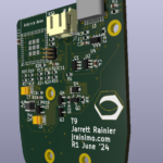
For the microcontroller, I’m deep in with the ESP32 ecosystem lately, and it hits all of the requirements for this project, so that trend will continue. I used an ESP32-C6 module that is tiny, has its own antenna, and the C6 has a Bluetooth stack. Also, USB serial/JTAG, as a bonus.
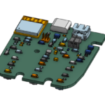
PCB:
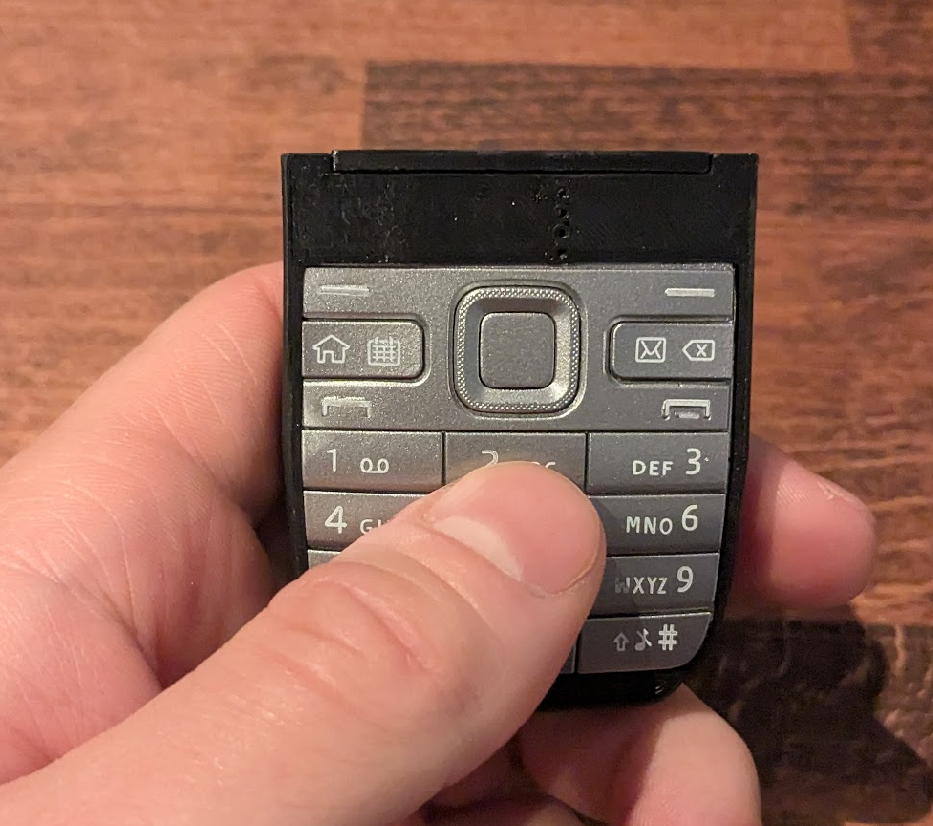
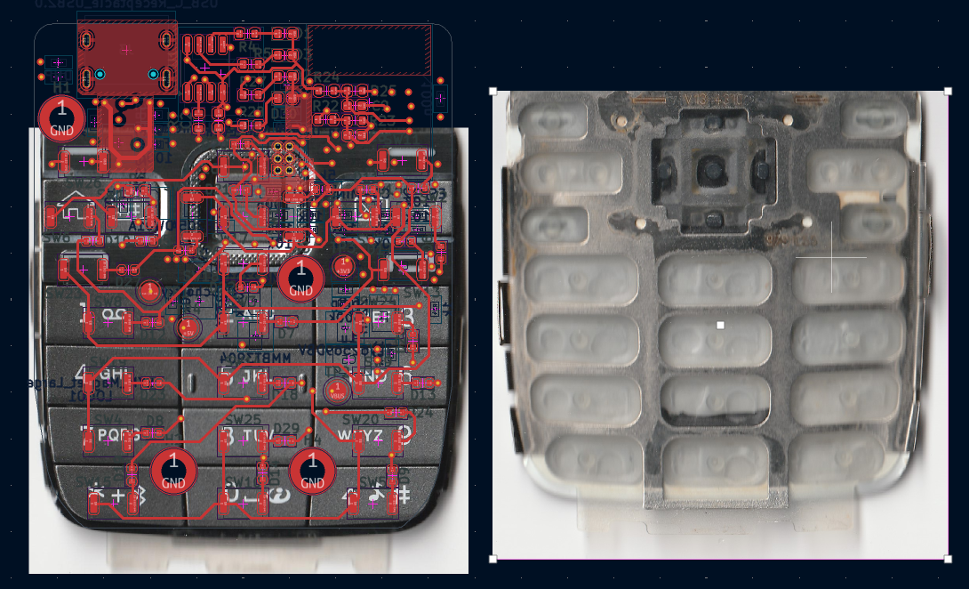
I built this up over the existing keypad of a Nokia E52 phone.
First, I scanned in an image of the keypad, then laid out my button arrangements in the proper positions.
This design was really irritating to solder by hand. On one side of the PCB, I have an array of 25 switches, that must be installed flat and level, and has melty plastic bits. On the other side, a large module with hidden ground pads. With both scenarios, I’d rather use solderpaste and a hotplate to get them on the board. But I can only choose one.
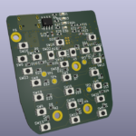
I used the hotplate to solder the switches, and then hot air and soldering iron to do the other side, which comprised of the majority of components on the PCB.
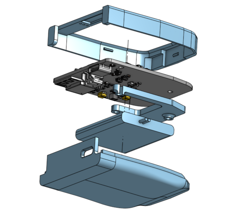
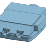
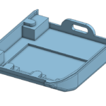
Enclosure:
OnShape, as usual for my personal stuff. I wanted a snap-together case that felt good in the hand.
For the mechanical CAD, I lofted a 2D profile along the edges of the PCB outline to build up the form. That was mostly an experiment in a new-to-me way of building up enclosures. It worked in that the final product was fairly organic feeling and looked good, but wasn’t very amenable to changes down the line.
Firmware:
Fun side story:
The last time I worked with Bluetooth in any sort of capacity was in 2013. I wrote an Android app for my Galaxy S2 that talked to a Raspberry Pi over a BT dongle. On the Raspberry Pi, I wrote software that controlled my Canon DSLR over USB.
It worked kinda well for a bit, until, adding features and piecing together my BT code from preliminary, incomplete specs, I probably made some invalid call. The BT portion stopped working, and never worked again on that phone.
Although being a little gunshy, I’d have hoped that Bluetooth stacks would have gotten a little more stable in the intervening years. I am only doing well-documented, reasonable things in this project (eg. Not trying to roll my own video streaming over BT), I have not yet bricked any BT stack, which is a good start. However, if I start flashing my ESP32 while it is paired with my phone, my phone (a Pixel 6A) crashes and gets stuttery until I restart the phone.
Bluetooth: Still extremely unpleasant to work with.
Other than bugs in the Android BT stack (I assume), the firmware is pretty straightforward. The ESP32’s NimBLE BT stack is well documented and easy to read and hack on, if a little verbose.
Slightly challenging was the state machine for the T9 keyboard logic. For testing, before I had my prototype hardware in hand, I was using an ESP32 devboard with no buttons. That means that with a significant part of my firmware design, I was typing numbers into a serial console, which was being sent as numbers to the microcontroller, converted back into letters, and then sent on. Kinda funny.
Version 2
First versions of electronic projects are never final versions.
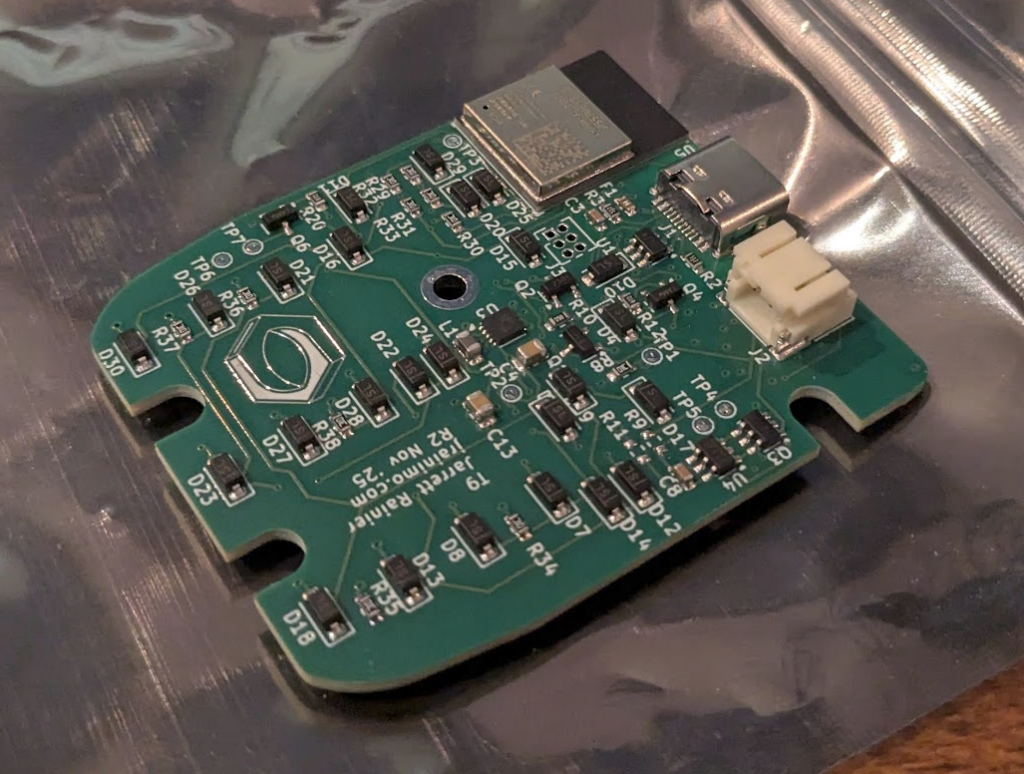
Good quality boards. The smallest features are the USB-C pins, which are soldered perfectly. My silkscreen on their is about the limit of what they promise to do, but as you can see, it should be totally possible to push the limit a lot more to keep the silkscreen legible while being way smaller.
PCBWay is really really consistent about their manufacturing/shipping times. As long as you can stick to parts that can be purchased within their region, full PCBA is like, two weeks. I cannot rant enough about how mindblowing that is. I really do like them a lot.
The essential changes I made are:
- The switches are higher force
- The ADC inputs to check battery and USB voltage are now gated, so they don’t provide a phantom power drain
- Slightly higher fuse current – 500mA was almost what an ESP32 can pull just during normal operation, if power save modes haven’t been enabled
- Added a vibration motor (C2759981)
- Changed the buck converter into a buck-boost
- Changed the battery charger to a SMPS design instead of linear
- Changed the DW01A to a PT8261
- Better mounting options for the PCB
One of the pain points of the first version is that it is very tedious to solder 26 tiny buttons by hand, even, level, and without melting the plastic. And on the other side, the bottom pad of the ESP32 was hard to get at. So I needed to get this assembled, and while the per unit cost wasn’t high, I didn’t want to pay for five of what was essentially a joke. PCBWay did me a huge solid though, and helped me out. I use them for most of my projects anyway! I love them.
People kept asking me why I used a buck converter on the first version instead of a buck-boost. The answer is that a buck-boost is a little less interesting to implement, a little more expensive, has a couple more modes that have to be tested, and only nets you about 17% more energy sucked out of the LiPo below 3V or so. but fine, added.
One feature I couldn’t quite fit in was an external memory chip. That would have enabled a proper T9 keyboard style, instead of just ABC. T9 requires a dictionary of the language in use, which for English, is about 30MB. Flash memory is physically huuuge. At least in the process size I could justify for this project, with the layer count I was at. If I went to 6 layers and finer feature size, then I could get away with it, but… Maybe… Version 3?
This PCB version came together really well. I didn’t have time to come back to V1 and fully swap out the DW01A, and… The replacement PT8261 didn’t work either. In this case, however, after spending an hour beating my head against the wall, I went to solder in the jumper bridge to remove the PT8261 from the circuit entirely. Where I then noticed that the PT8261 was powered through a 0-ohm resistor that I had never populated at all. Yeah, it was completely unpowered. After I bridged that footprint, it worked great!
The buttons no longer feel a bit spongy, and the additional hit of the vibration motor makes it feel wonderful.
I used a different technique for the enclosure design than in V1.
For the first one, I designed the enclosure AFTER I had finished the PCB so there were some oversights that required an extra little shelf for the battery and some metal locating pins that made installation fiddly. For the mechanical CAD, I lofted a 2D profile along the edges to make up the form. The result was very good, but the process was more art than science, and wasn’t good for iterating or making modifications going forward.
In this version, I designed both the PCB and the enclosure in tandem, with features in both working together.
I used the exported PCB as negative in the outer enclosure, expanding the dummy PCB and adding battery and dummy ports and keyboard and such to make it fully parametric.
-
- PCB
-
- Negative Mould
-
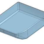
- Positive Mould
-
- Result
Honestly, I don’t like how it looks as much as V1, but that’s an industrial design issue, not a structural one.
And the project lives!