This is a pretty rare combo: using a premium PCB package with the budget board house.
Kinda funny.
Generally these small run PCB houses provide DRU and CAM files for EAGLE design rule checking and Gerber outputs, respectively. Because I’m using Altium, I had to make it up as I went along.
It gets much easier when you understand what Gerber files are. While we’re all used to standard, unified output formats that contain all of the data we need, Gerbers are very much still a holdover from manufacturing in the 80s.
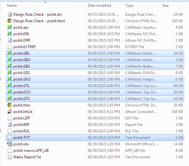
When you export these, a whole bunch of files get generated. This is intimidating, but don’t panic! They all have different extensions like GBO, GTL, etc. These are all the same type of file.
As I’ve said, while you’re used to unique file extensions being different formats, these are a holdover from 80s manufacturing and the PCB industry still hasn’t caught up. That means that by changing file extensions, you can play around with different layers doing different things.
So here’s how you generate the appropriate Gerbers. I used a mostly the default rules for this, I’m not pushing the limits. Maybe next time I’ll generate the proper rule sets.
Read and understand these directions before you start. They require some forethought.
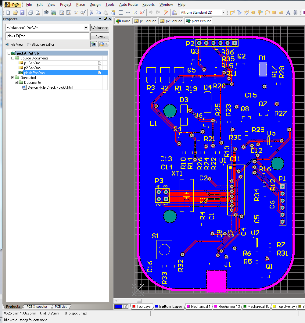
Start out with your finished PCB.
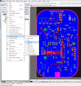
Do the thing.
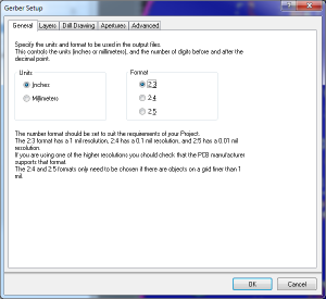
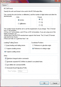
The resolution options matter here. There’s no way Dirty PCBs can handle the higher res, so turn it down a notch.
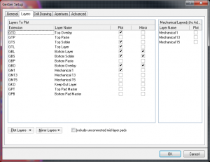
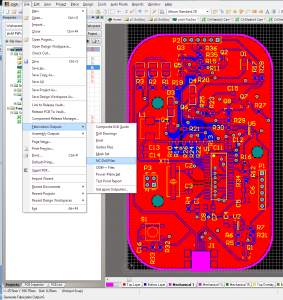
In the next tab, this is where you’ll have to do some thinking. Every project is slightly different. So for this one, I want the top overlay (silkscreen), top solder (gaps in solder mask for your pads), and top layer (copper). Same thing for bottom.
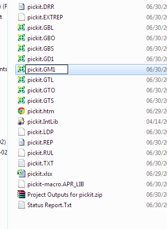
You also need a board outline. Older versions of Altium don’t have a dedicated “outline” layer, although I believe newer ones do.
So what I did was change the board outlines to Mechanical 1, and now I’m exporting that.
A couple more notes:
If I wanted to create a solder paste stencil, I would also export the Paste layers.
If you want through-hole slots, you will need an additional layer. This includes slots that allow you to panelize. Export them on another mechanical layer, and I’ll talk about it a little later. I’ve done this before, DirtyPCBs does a great job of this.
All of the other tabs in this dialog are kept at default values. Don’t mirror the bottom layers as shown. I did that and it was Wrong.
I lied a little bit above. Of the exported files, there is one that is not like the others. The drill file (.TXT in this case) requires it’s own export.
Do the resolution thing again, and everything else is default.
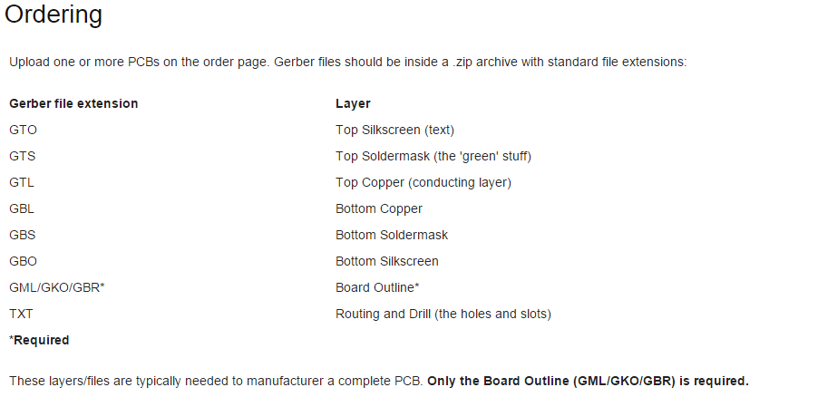
Okay! Now we’ve got all the files we need, let’s make sure they’re in the order they need. Here’s the key on the DirtyPCBs website.
As you can see, it’s super similar to what we have. The top 6 are exactly what we exported, and the drill TXT, too. The outline is the only thing that’s not quite right.
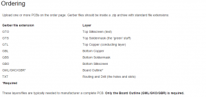
We exported it this time as mechanical layer 1. Easy fix, just rename the GM1 file to GKO. If you’re doing internal slots or self panelizing, you’ll also have exported another mechanical layer. Say, GM2 or GM15 or anything you like. Rename this to GML and include it with the others.

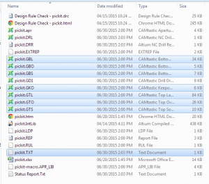
And there you go! Zip up all of these files, and they should turn out alright. GD1 is the Gerber drill file that this board house doesn’t use, just ignore it.
An important step: Check your files.
CircuitPeople is an excellent and simple online Gerber viewer. Look at all your layers and make sure nothing is terrible.
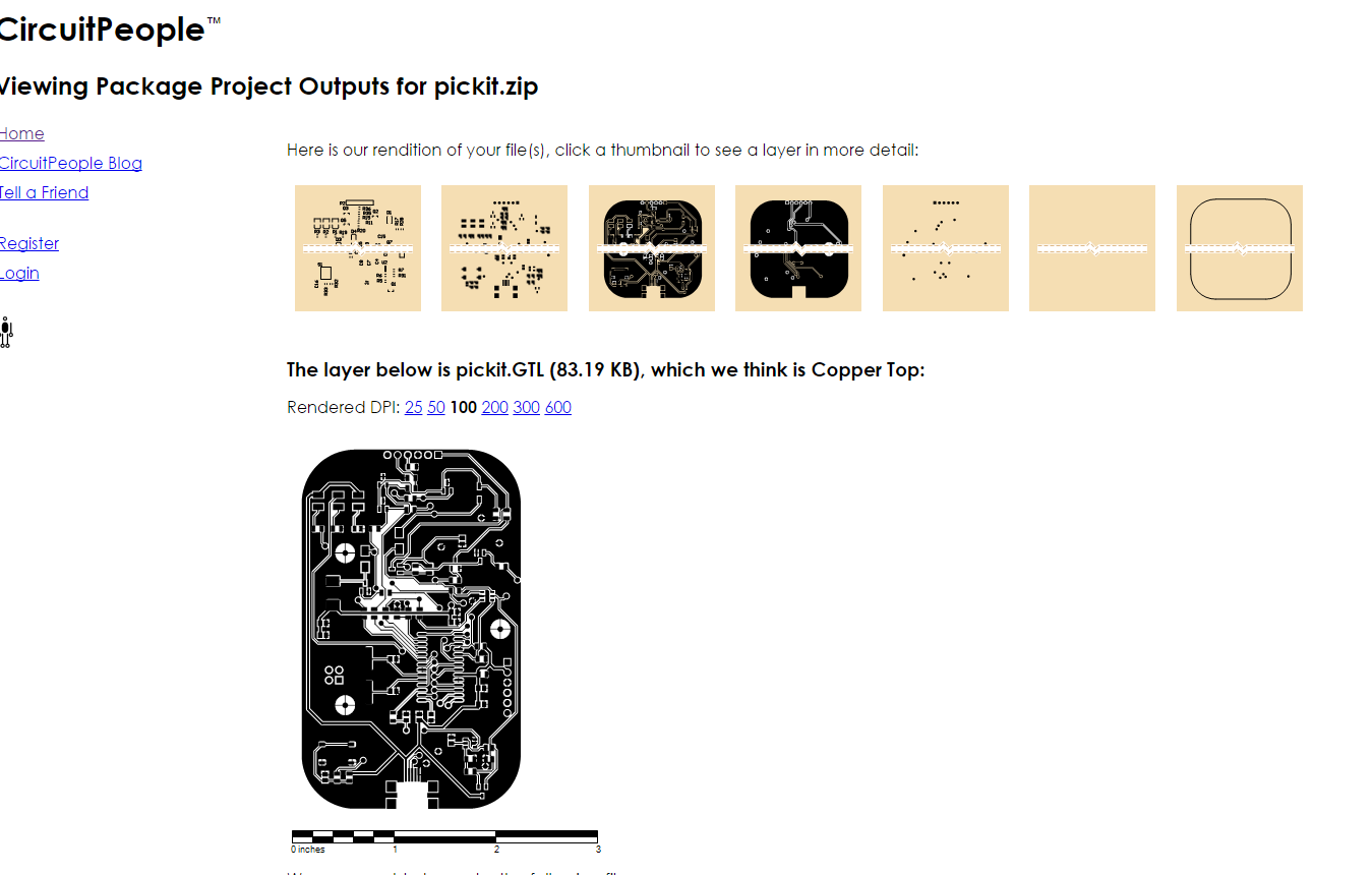
And you’re done! Send it off and enjoy your boards.
If something screws up in the order, I’d like to hear about it, but I take no credit. These steps have always worked for me, but this particular company probably won’t tell you if anything is wrong with the files. They’ll just manufacture it and send it on.