Archive for Quick Tips

Force-Directed Circuit Board Footprint Autoplacement

From Wikipedia:

Force-directed graph drawing algorithms are a class of algorithms for drawing graphs in an aesthetically-pleasing way. Their purpose is to position the nodes of a graph in two-dimensional or three-dimensional space so that all the edges are of more or less equal length and there are as few crossing edges as possible, by assigning forces among the set of edges and the set of nodes, based on their relative positions, and then using these forces either to simulate the motion of the edges and nodes or to minimize their energy.

Force-directed graphs are a common way to display things like mind-maps. It’s a good way of spreading out the whole collection, while grouping related items together, and minimizing the path length between the closely related items. In my mind, this has a lot of similarities with how PCBs are laid out.

Well, there’s only one way to prove that theory.

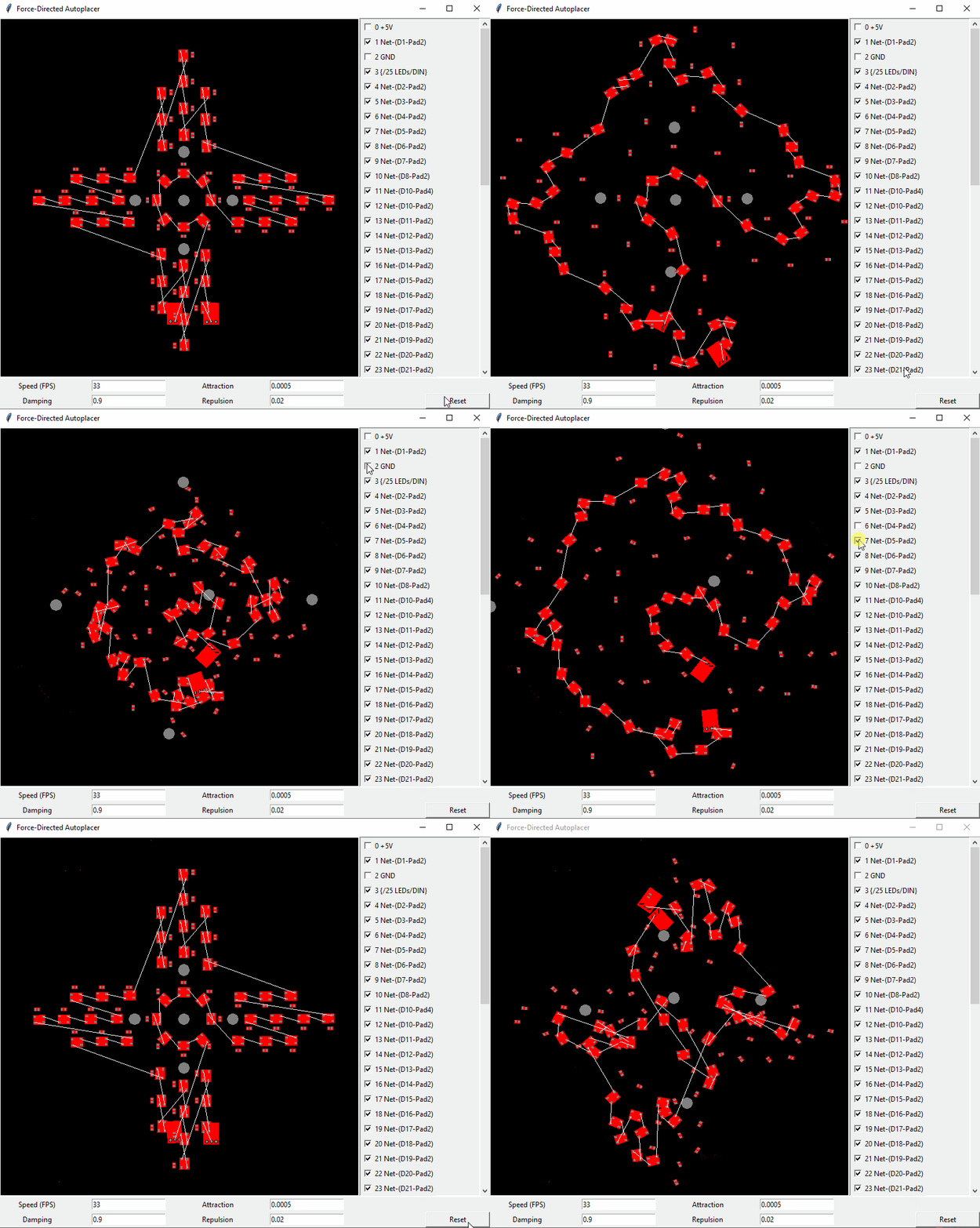
KiCad Footprints animated in an exploding fashion

Using KiCad PCB parsing code I wrote for another project, I was quickly able to grab the nets and footprints out of a KiCad project. Displaying the nets and allowing specific ones to be turned off was a feature I identified as critical early on, because the ground or power nets would overwhelm any of the others, rendering the important nets useless.

Truthfully, a significant part of this was wrangling TKInter to build the Python GUI that I wanted. It was a success, but I’ve never used it before, and I am not a fantastic UI designer.

Under the hood, the system essentially treats each of the nets as a spring, and applies a simplified version of Hooke’s Law to each connection. Each of the centre point of the footprints acts as a charged particle, and a simplified version of Coulomb’s Law acts upon it to repulse all of the other footprints. These algorithms are a pretty typical way to do this, by essentially setting up a physics simulation. One tweak on this strategy that is unusual, is that the nets don’t act on the footprint origin. They act on the pad itself, which allows a torque to impart a rotation on the footprint.

I’ve gotten this project as far as “fun tech demo”, and it’ll likely fall dormant for a while in this state. At some point, I will build an appropriate PCB using this technology, because I love making unusual designs that are electrically fine.

The repo is here. Have at it.

Dumping Firmware With a 555

Voltage glitching, also called fault injection, is the process of dumping the energy on a microcontroller’s power rail very briefly – Just enough to cause a glitch, where it skips an instruction, rather than causing a brown-out-induced reset.

I first learned about the technique in connection with the Chip Whisperer, which is an FPGA-based board with all the bells and whistles. It’s quite expensive, and like any other situation where you add an FPGA, very complicated. Naturally, that has elevated it to a level above what mere mortals can perform in the limited free time we have.

After knowing about this, and having it in the back of my mind for several years, I finally have a good use-case that can justify spending some time on this. I have a pile of generic STM8-based devices, and while I have written some of my own alternative firmware, I’d love to be able to dump the original flash to revert them back to factory code.
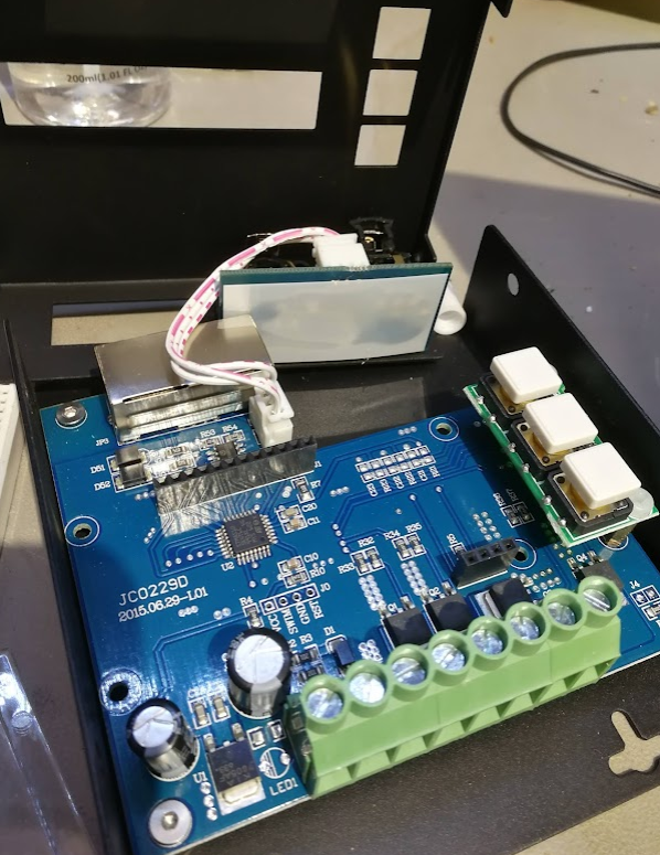
The function of the device doesn’t matter, that’s not the point of this exercise.

Some quick searching for options leads to this recent write-up, which is sparse on details, but serves as excellent inspiration that this task is very doable.

A few architecture notes:

The STM8 has a Read Out Protection bit in the configuration area of its flash memory. When the programmer attempts to read out the flash memory, the bootloader first checks this bit, and if it’s cleared, it starts reading out the flash to the programmer. If it’s set, it just reads out zeroes. Write capability is never blocked – That is, you can still write a zero to that ROP, and then the microcontroller will be “unlocked”, but it does clear the program memory, too.

One of the pins on STM8s is called VCAP, and it’s attached to the internal voltage regulator. The CPU runs on this voltage rail, not the actual voltage that is provided to the IC’s power pins. The pin is intended to be connected to a decoupling capacitor, and that provides an perfect spot to inject my glitches. Most microcontrollers also have something called Brown-Out Resets: When the input voltage rails sags too low, the peripheral triggers, and resets the microcontroller. Obviously, this is something we want to avoid, and using the VCAP pin should help with that.

In terms of glitching, there are two important considerations:

The glitch must start at the same time or during the cycle in which the CPU is trying to read the ROP bit, and the glitch must not last long enough to trigger the BOR or to make any other important instructions fail. It’s not easy to know these exact timings, so any reasonable values must be tried, essentially brute forcing the process.

Now, the logical way to do this would be to use an external microcontroller to wait for the programmer to reset the system, wait a set period of time, and then trigger the output transistor to glitch the voltage rail. That’s boring! You know what else can do that? That’s right, a pair of 555s.
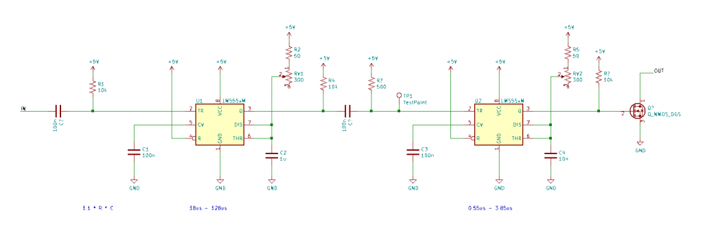
Here are two 555s set up as monostable pulse generators. The input is the RST line on the STM8 programmer. The first 555 then sets the delay. The second 555 sets the length of the output pulse. Both of these timings are controller by a different potentiometer. These then go to a MOSFET that dumps the energy stored in the internal voltage regulator cap.
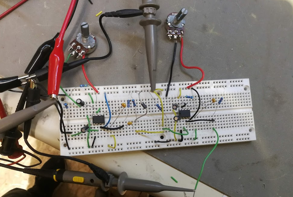
After building it with larger-than-designed time values and testing it to prove that the waveform looks as expected, we solve the next hurdle:

To figure out decent ranges for the potentiometers, my STM8 board runs at 8MHz, which means that each clock cycle takes 125ns. The STM8 requires at least 2 clock cycles for each instructions (one for retrieval and one for execution), and more for instructions with multiple bytes or arguments. So, ballparking, we need a pulse that’s anywhere from 0.2us to 1.2us or so.

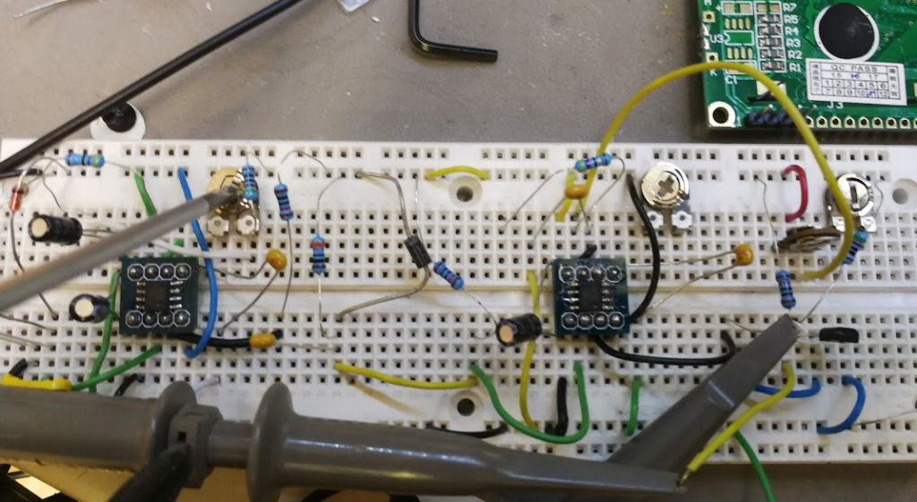
One problem with a typical 555 is that it can only generate pulses as small as 10us. Fortunately, I have a pair of high speed versions up my sleeve, the LMC555. It has a 10ns minimum pulse instead, which is very zippy. They’re SMD only, so they get popped onto a breakout board to fit the breadboard, and replaced. Some other components got tweaked too, as I played around more.
 

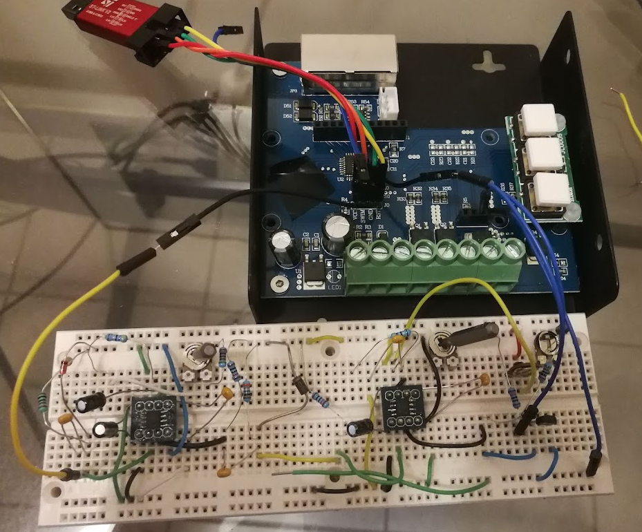
Now on to the programmer. I’m using a standard STLink V2, which speaks the SWIM protocol that allows programming and reading of the STM8’s flash.

With a little bit of bit of Python and stm8flash, we get this:


import subprocess
# .\stm8flash.exe -c stlinkv2 -p stm8s105?4 -r out.bin -b 1
out = b'\x00'
while out == b'\x00':
subprocess.run(['stm8flash.exe', '-c', 'stlinkv2', '-p', 'stm8s105?4', '-r', 'out.bin', '-b', '1'])
f=open("out.bin","rb")
out = f.read(1)
print(out)
subprocess.run(['stm8flash.exe', '-c', 'stlinkv2', '-p', 'stm8s105?4', '-r', 'out.bin'])


In PC applications, writing text to console is a surprisingly slow process, so a low-effort tweak I made to make the loop run faster is to remove the flash utility’s console logging, just by removing some lines here.

So, all set up, potentiometer on the left controls the delay, pot on the right controls pulse length.
And, bam.

Firmware dumping with a 555.


Well, not that fast. It took about 45 minutes of fiddling with the knobs until all its secrets were unlocked. I’d sweep the right knob the whole way, then tweak the left knob very slightly, then sweep the right knob again. It only really worked because the knobs only had to be within the right range for a very brief period of time. It only had to work once.

Would this have been easier with a microcontroller? Oh yes, of course. But that’s not nearly as interesting.

Chromaticity

Here is a brief overview of how light and colour work, in the context of LED lighting.
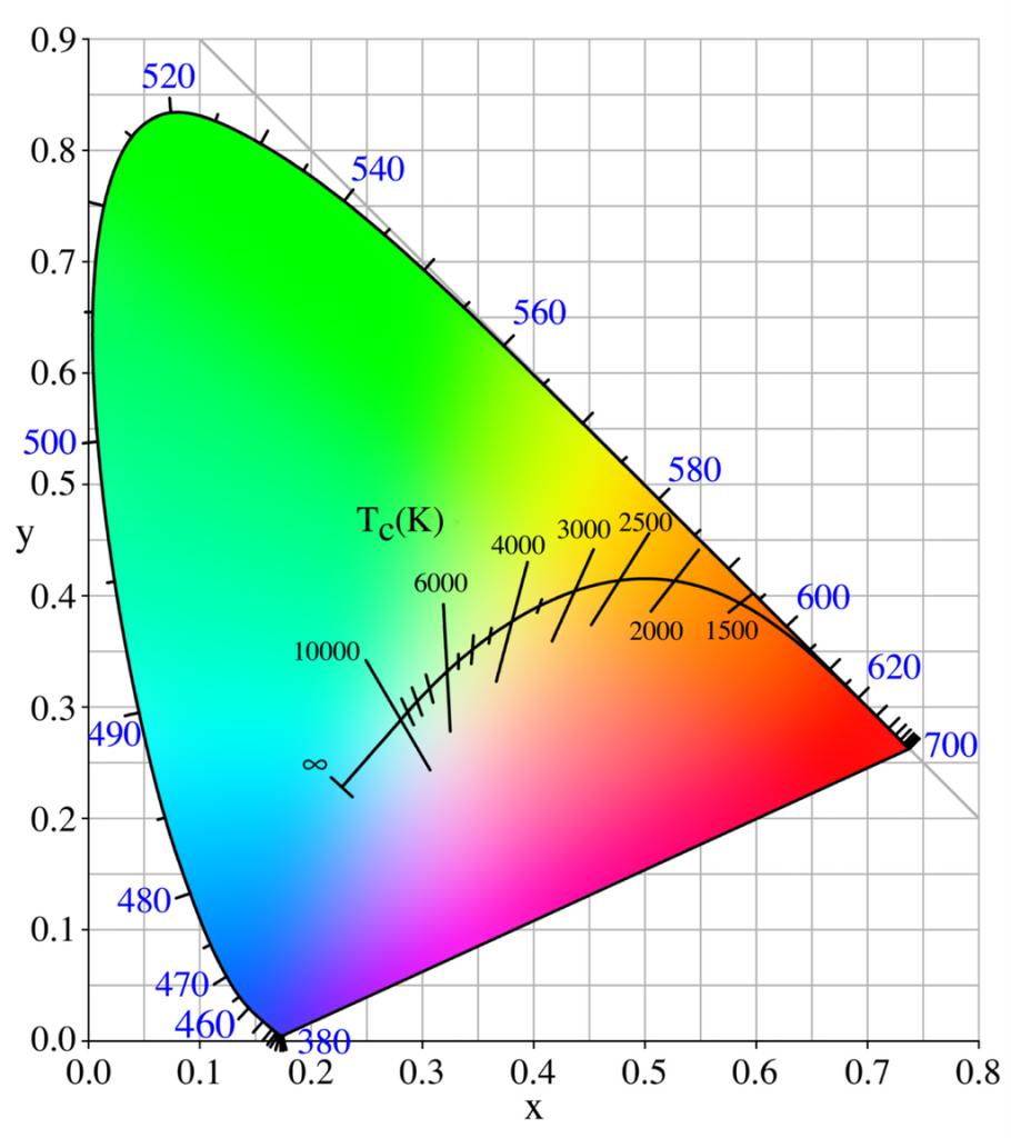
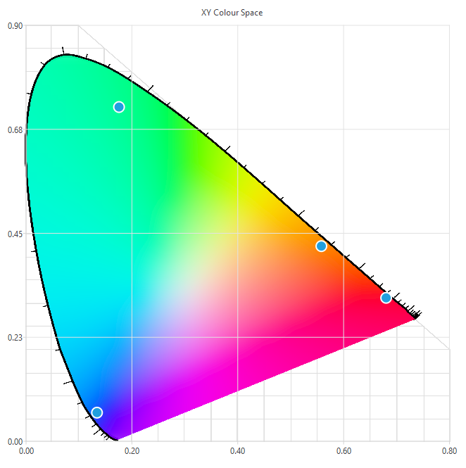
We’ll mostly be discussing the CIE 1931 colour space, with reference to the chromaticity diagram, shown below.

This is the 1931 version. Newer versions that look slightly different have come out, but the general intent is the same, and they are all used for different calculations. The 1931 version is “good enough” and is universally the one that is referred to when a colour is described in xy coordinates.

The points along the edge are pure visible wavelengths (displayed in nanometres). Anything inside the diagram is some mixture of the wavelengths.

Computer monitors don’t have the same kind of visible range as your eyes, so the colour space diagram above is just a representation, not the actual colours that you would be able to see if it were displayed side-by-side with the actual light wavelength.

There’s a curve along the centre, called the black body curve, that represents “white” light. White can be many different things – Typical incandescent bulbs are around 2500K, towards the right (warm) side of the black body curve. Daylight is very cold, with lots of blue components, towards the left. As long as it’s along that curve, it can be considered “white”. The vertical-ish lines indicate where that particular temperature extends, if a given data point isn’t exactly on the line. Duv, or “delta u,v” is a measurement describing the point’s distance from the line.

In terms of white LEDs, there will typically be a “warm white”, also called “tungsten”, and a “cool white”, called “daylight”. As shown by the black body curve, if you have both LEDs, you can’t interpolate between the two of them and expect the light output to follow the curve. It will be a direct line between the two. There are a couple solutions to this, and an easy cheat is to explore the strategy that one of the industry leaders is utilising.
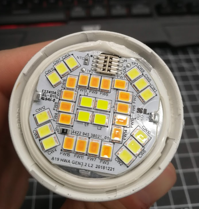
The Philips Hue tunable white smartbulbs are excellent. I’ve taken apart a handful of smartbulbs, and the Hue has the largest quantity of LEDs I’ve seen(read: brightest), as well as using a few tricks to get better light quality than any other system I’ve seen.

The daylight LEDs, labeled “CW”, and tungsten LEDs, in this case labeled “FW”, (we’ll get back to that) are fairly standard. In the centre is where it gets interesting, with the LEDs labeled “L”. This is lime green.

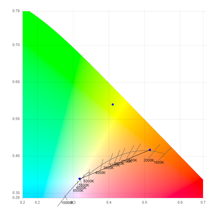
Here is a closeup of those LEDs plotted on an XY graph, with the black body curve, and an interpolation line between them:

With both of the tungsten and daylight LEDs located on the black body curve, fading in between the two will drag the light significantly away from what we perceive as “white”, essentially making the light look magenta. The lime LEDs, towards the top of the graph, are perfectly situated to pull the light output back onto the curve when the bulb is at an intermediate temperature. Some further investigation into the meaning of the LED designators on the PCB, “FW”, reveals that some LED manufacturers with that particular temperature of LED call it “flame white”. It’s substantially warmer than most bicolour white LED tapes, at around 2200K. Mint LEDs are also sometimes used for the same purpose as lime LEDs. Mint has similar spectral components to lime, but with a little more blue components, moving their xy coordinates a little more towards the bottom-left.
Here they are next to a high quality warm/cool (bicolour) LED tape:

From left to right: my daylight, Philips daylight, my tungsten, and Philips flame. Daylights are fairly similar, within binning and measurement tolerances. My tungsten LED is 2600K, showing how far the Philips flame LED is into the red spectrum. Another strategy for getting temperature that warm is to add an amber LED.

Tungsten, flame, and amber, left to right respectively:

Tungsten LED can be combined with amber to get a warmer (lower) temperature. Amber has an additional purpose: Standard RGB gamuts don’t have a whole lot of range in between the red and the green colours, which can be filled out with the added amber channel. More on this in a bit.

“Gamut” is the displayable area made possible by mixing the available colours. Displayable points drawn with each primary colour, and the available gamut is any point within the area.

Here’s a typical RGB LED tape.

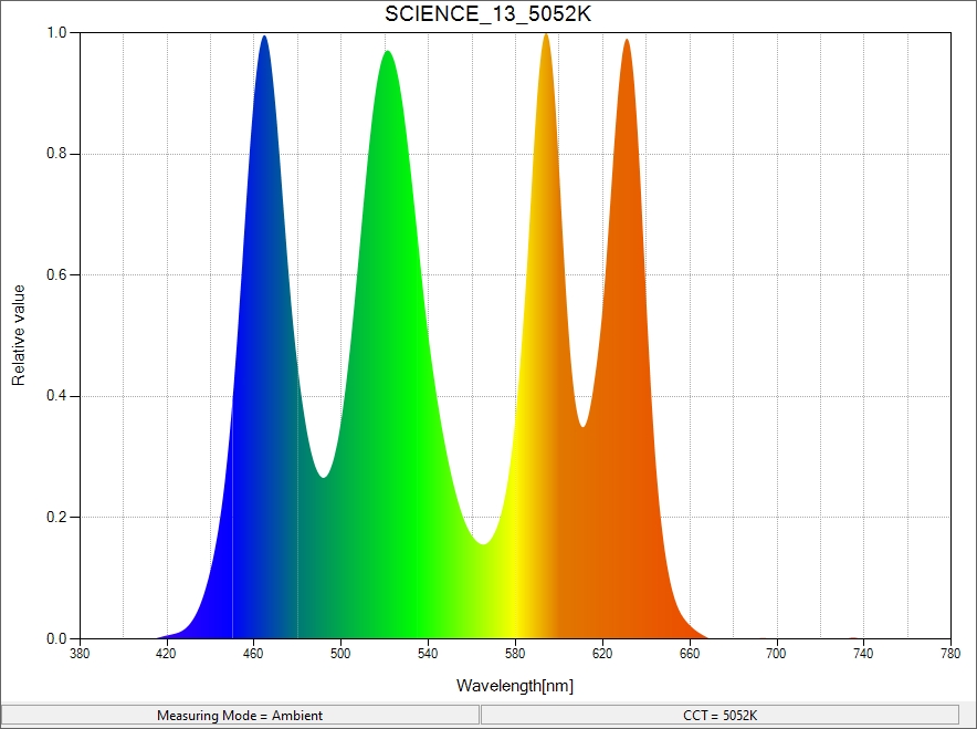
And their spectral distributions:

This green has a slightly wider spectrum than the other primaries, so it doesn’t fit as nicely on the edge of the xy graph. It’s made up of mostly 520 nm and 540 nm components.

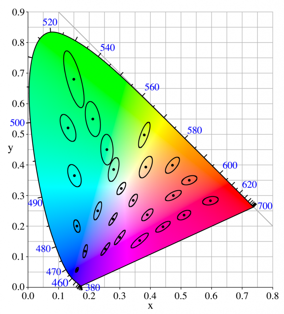
The MacAdam ellipse is a graphical representation of what observers see as “one colour”. That is, anything in the ellipses shown appear to be the same colour to a regular person. This particular image is only the results from one participant in the study, so it shouldn’t be taken as definitive, but it does show trends that can provide actionable insights. The shapes are also exaggerated by about ten times for ease of clarity.

The ellipses tend to flow in the direction of the blue-red line, for example, showing only a few different perceptible shades in between those two primary colours. Red to green however, particularly in the red to yellow region, are extremely granular. This is where amber comes in.


The amber gives additional granularity in the existing gamut region where our eyes are very sensitive, and in the space where the gap between the RGB peaks is largest.

Emerald green, at 560nm, is another LED that would help fill out the spectrum gaps, providing more range towards the green part of the red-green line. Emerald and amber doesn’t alter the overall gamut significantly, however. There are areas without coverage on all sides of our gamut triangle, but the area to the left of the blue-green line is the most significant. This could be supplemented by InGaN cyan LEDs, at 505nm. That will be the topic of future experiments.

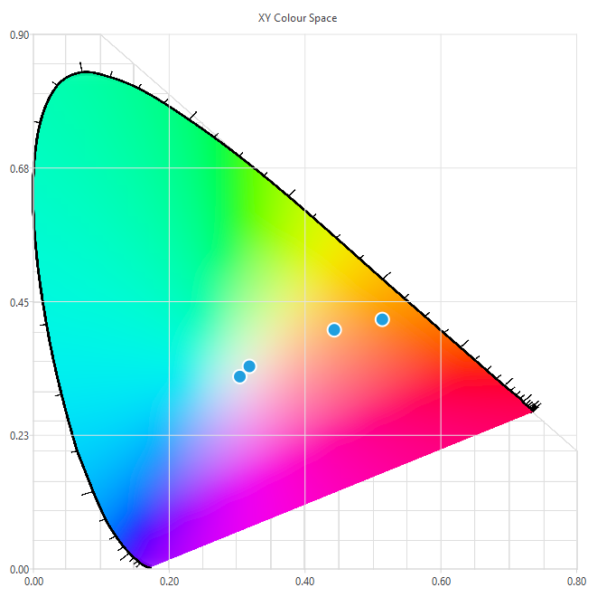
For reference, here is a graph of all of the colours measured and discussed.


LiPo Systems with USB Power

I’ve alluded to this in the past, once or twice.

Power management in battery applications is pretty tricky. There are a lot of different situations, and a lot of different strategies. In the past, for the topic of this conversation, single cell Lithium polymer batteries, I’ve used a pair of Schottky diodes to automatically “select” the highest voltage feeding the system. That will be either 5V USB power, or 3V-4.2V LiPo battery.

It was suggested to me to use the body diode of a P-Channel MOSFET, but I dismissed that as unnecessary: the body diodes have no lower voltage drop than a Schottky, around 0.2V. Here is one of the more readily available results for battery/wall-power switchover:

https://electronics.stackexchange.com/questions/105053/li-po-charging-circuit-question-switching-between-battery-and-power-supply

That thread doesn’t make a good case for the FET solution over the diode, but the initial suggestion to me indicated that, once “on”, MOSFETs will conduct current in either direction. This breaks my understanding of how they work, but it warrants more research.

That search on its own is confirmed by:

https://electronics.stackexchange.com/questions/48646/in-an-nmos-does-current-flow-from-source-to-drain-or-vice-versa

Stack Exchange posts don’t make for good engineering, though. This calls for a simulation!

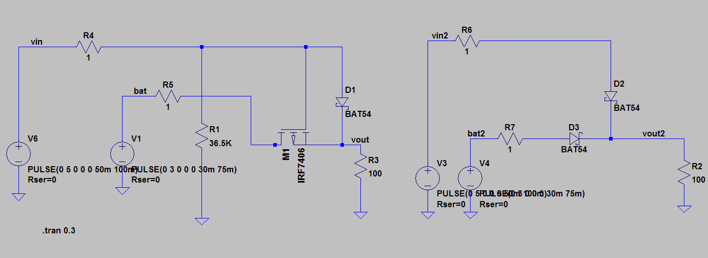
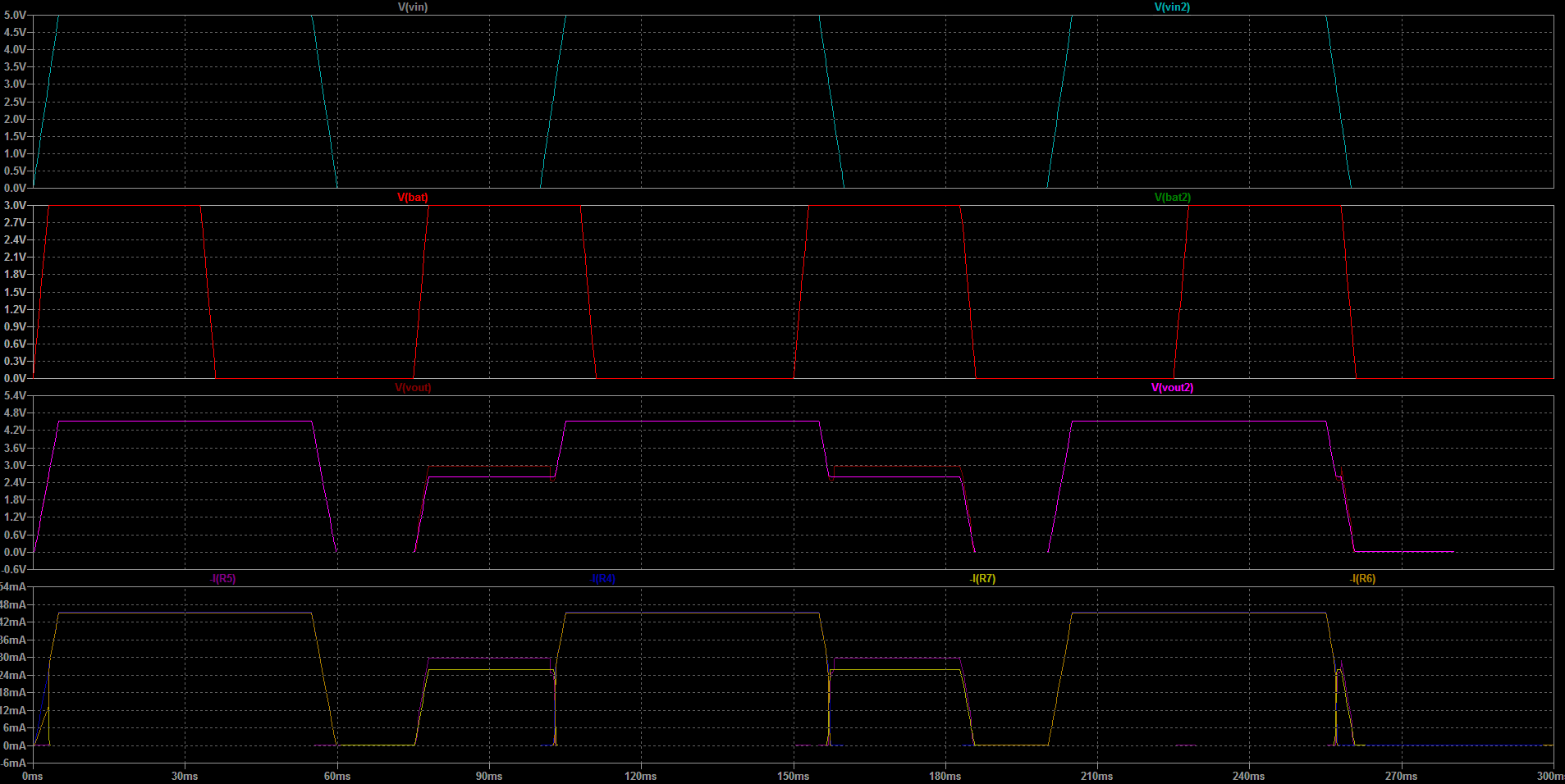
Initial results check out! Those output waveforms on V(out) and V(out2) should be identical, if the current through M1 was purely through the body diode.

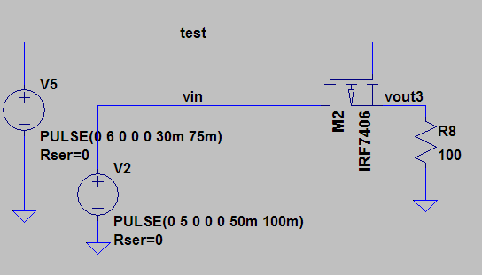
Simplifying this even more, we can do this:

That results in the following waveforms. You can clearly see the shoulder in V(out3) (blue), where the MOSFET transitions from conducting through the body diode, to conducting through the transistor junction itself:

That’s pretty conclusive. It’s weird to find gaps in my understanding of basic electronic building blocks at this point, but I’m always on-board with more education.

So now this is a documented solution at handling the power switching circuitry between USB and lithium batteries.

In the future, I should put together a written record of the strategies for charging the LiPo batteries in the circuit, and also low-voltage cut-offs to avoid over-discharging and permanently damaging the batteries.

PicFix

Here’s an issue that was causing me some grief:

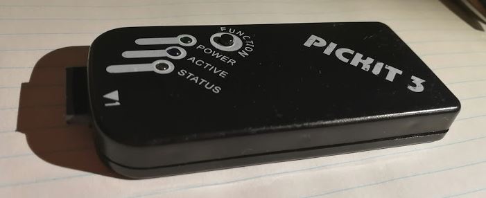
In newer versions of MPLAB X, Microchip’s IDE, My PicKit 3 clone wasn’t able to supply power anymore.

Some investigation revealed that in MPLAB 8 and before, they didn’t used to properly check for “correct” voltage before attempting to continue programming. Which is great! But they fixed that.
Here’s the message it displays:


PICkit 3 is trying to supply 3.250000 volts from the USB port, but

 the target VDD is measured to be 2.875000 volts. This could be

 due to the USB port power capabilities or the target circuitry

 affecting the measured VDD.


The target circuit may require more power than the debug tool

 can provide. An external power supply might be necessary.


Connection Failed.


Cracking open the case reveals that it’s made by Sure Electronics, and there was possibly some nebulous licensing deal with Microchip to sell these, and then they got cloned and the deal evaporated. Or something. It’s hard to tell.

Oh look, a schematic. Relevant schematics on page 69 and 70.

I had a sneaking suspicion that there was a bad voltage divider somewhere that was causing ADC readings to come back too low.

Before having to properly poke around, this post confirmed my suspicions and made things super easy.

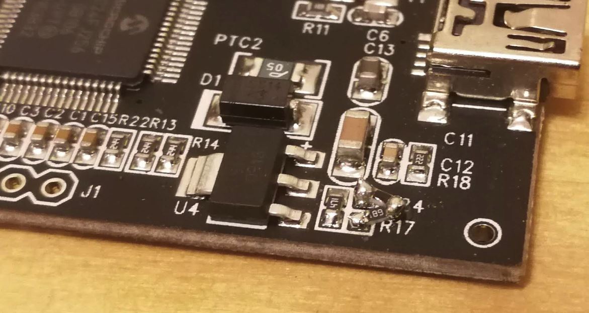
Near the linear voltage regulator, the AMS1117, there are two resistors named R17 and R24. They are 470 and 680 ohms, respectively.
Swapping the 680 ohm resistor with a 750 ohm is recommended. I didn’t have one, so I desoldered one leg and put a 50 ohm resistor in series, making kind of a tower on my board. Results in 730 ohms, but it seems to work. My PicKit can provide power again!

Storytime! A switch mode tale.

A lot of the switch-mode power supplies I’ve built have relied on Skyworks Technologies controllers. This is because they are very cheap, and seem to go obsolete almost immediately after purchase.

This is a quick story of bringing up a new switch-mode circuit from a different manufacturer to test its viability in some battery-powered devices.

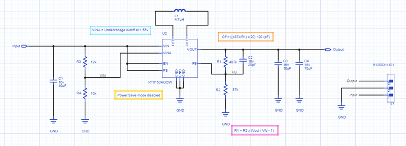
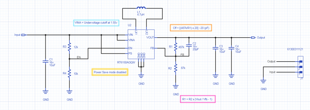
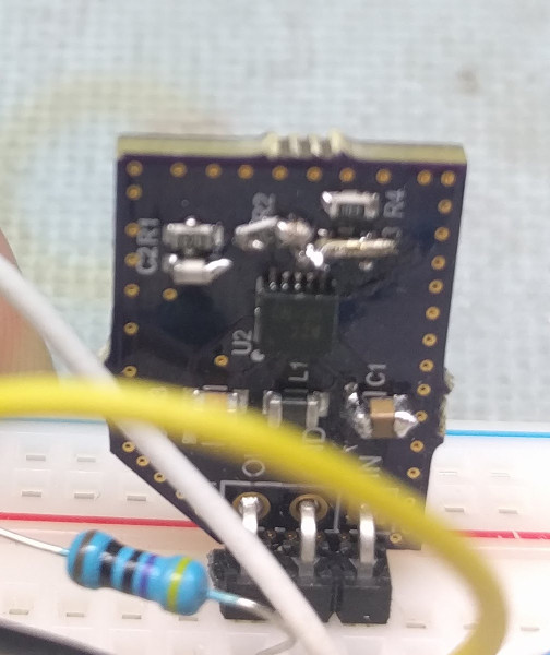
I’m using a Richtek RT6150A buck-boost controller.

For a 3.3V output, buck-boost topologies are necessary when the input is a LiPo battery. The ~3.0-4.2V safe voltages for charge and discharge are perfectly bracketing the 3.3V target in a way that is about as inconvenient as possible.


Other than cost, the reason that I selected this chip was that it seemed marketed towards this exact application. Battery technology is written in the advertising materials, and the datasheet shows this:


Oh yeah,  perfect! An undervoltage cutoff. That should be good for LiPo protection.

so I drew a schematic like this:


And then sent it off as a one-off PCB through OSHPark.

It costed about a dollar.


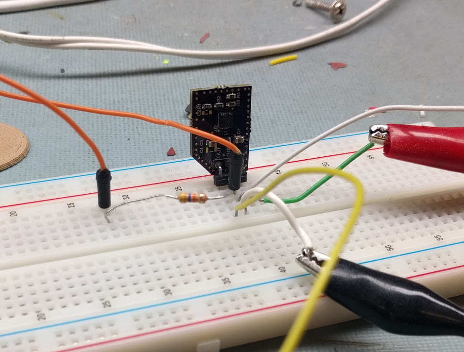
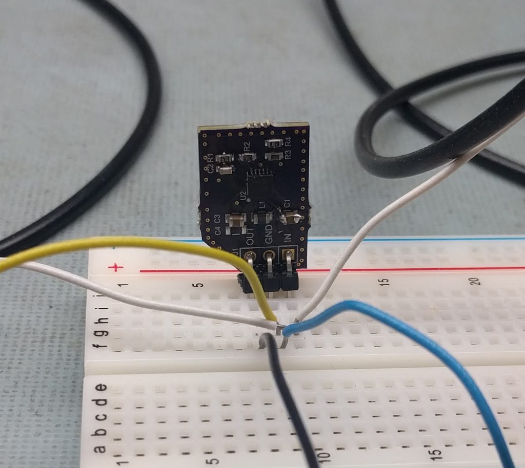
I got it back, soldered it, and did a quick bench-test. Instead of cutting off at 3.3v like I intend, it didn’t turn on until close to 5v.

No good!

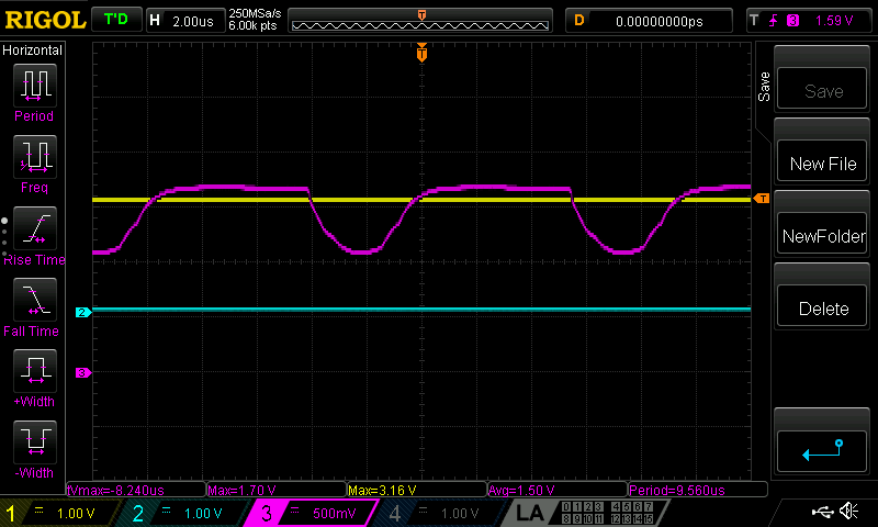
So I pulled out the scope and checked the voltage at VINA:


The input voltage was completely stable, so that wavy portion in the middle of the voltage divider wasn’t coming from the input.

Going back to the datasheet:


This was ambiguous, but hindsight tells me it’s not actually intended to be a voltage cutoff. This is just the power for the control circuitry itself.

What was happening was that the internal control circuitry was drawing enough current that the voltage at the middle of the divider sag enough that it hit its cutoff, and turned the chip off, making the voltage rise enough that it turned on again, etc.

This chip is advertised in Richtek’s appnotes as being good for LiPos because of that cutoff, I assumed, but it doesn’t actually work!

So, I bodged VINA to VIN, and now it works, albeit at the full range of the chip. That’s not exactly what I want.

The other thought is to use EN as the cutoff.

It’s supposed to shut the chip off at “logic level low” whatever that means for a wide input voltage chip.


Logic level is anywhere from 1.4 to 1.8v, which is annoyingly wide.


But I gave it a shot.


Some test results:

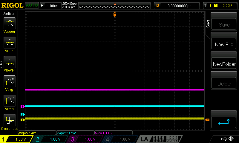
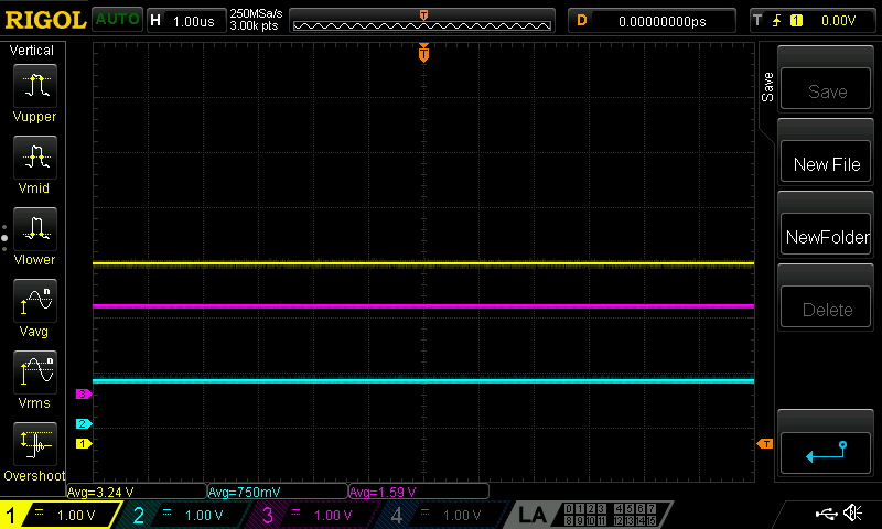
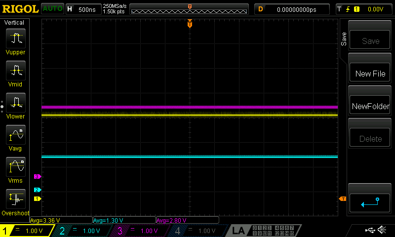
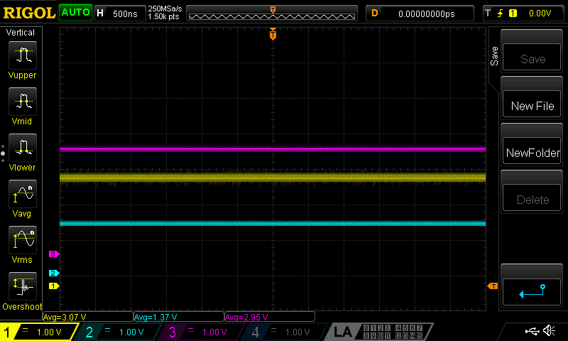
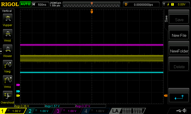
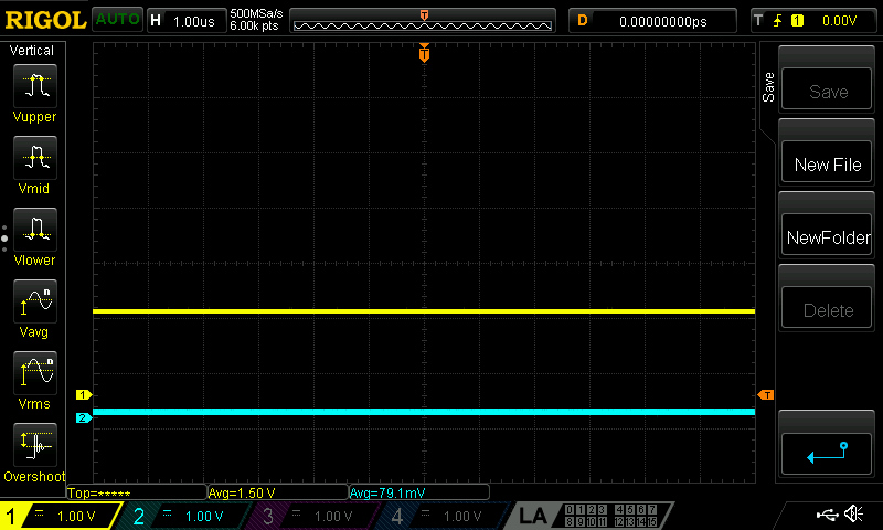
Channel 1(Yellow) is output, 2(Teal) is the EN pin, and 3(Purple) is the input voltage.

At 1.11V input, output is still disabled.


At around 1.59V, the output springs up to 3.24V:


Weirdly, as the EN pin gets closer to the theoretically 1.55-ish point where it’s supposed to turn on, output noise starts to hugely increase:


Until right at the logic level high point, the output voltage has almost a full volt of non-periodic, constant noise:

It’s possible that it’s not a coincidence that is right when the controller switches from boost mode to buck mode.

So again, let’s bodge this back into a manufacturer-recommended specification:

Replacing R3 with a 0-ohm resistor (or: a wire) gets this back into spec:

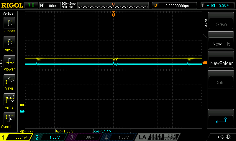
In this case, the output (teal) is still disabled until the input(yellow) starts to hit 1.50V.


From there, there’s a sudden switch-on at 1.56V to 3.2V output:


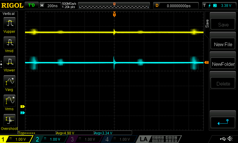
And it quickly rises to a 3.3V and stays there for the full range, up to 5V input:

Output ringing is a periodic 1V peak-to-peak for about 20ns, every 1us or so. This gets a little lower when the output is loaded and provides some damping.


So the moral of the story is that the Richtek RT6150A works quite well, but only when the datasheet is closely adhered to. Anything “interesting” in the design leads to unacceptable noise or unpredictable results.


In the meantime, the RT6150A seems to be on the way to phasing out. Stock on Digikey is 0, with a 16 week lead time for new parts. The catalog not-so-subtly hints at using the RT6150B variant, and the datasheet is almost identical. The glaring differences are a few added lines in the marketing copy on the first page saying that fixed 3.3V operation is possible by tying the feedback pin directly to the output.

Anyway, that’s my debugging story. Nothing was particularly novel or unusual, but it was a good process to document irregularities while abusing the chip.

Rapidly Building Software to Prototype Quickly


TLDR: I wrote an Inkscape extension to make my life a little bit easier when designing assemblies with laser cutters.


For the most part, I avoid using 3D printers while rapidly prototyping. Until very recently, they have been little better than toys; unreliable, inaccurate, and high maintenance. The laser cutter, however, is a tool. By cutting and joining multiple sheets, three-dimensional objects are still faster and often better than 3D printed parts.

Additionally, when I’m trying to build something really fast, I find it much quicker to sketch out profiles in Inkscape than CAD them up. Inkscape is totally rad open-source vector drawing software, if you’re not familiar. Being able to see assemblies in 3D is nice, but I can do that in my head for quick and dirty projects.

One of the bottlenecks in this process that really messes up my flow is hand-drawing box joints. It’s tedious and error-prone to copy mating profiles that are dimensionally accurate.


But wouldn’t it be great if it only took two seconds?

So this is QuickJoint. It’s a simple Inkscape extension that will add box joints to selected objects.


This first version can do male tabs or female slots. The tabs by selecting a path, and then in the menu choose which side (and direction) to tabify.

The slots will use a single line as a guide, accounting for the laser’s kerf.


This is a work in progress. Fine tuning with how kerf computation works will be tweaked. Slots/tabs may be changed to autodetect so that everything can be done at once. There are a few more changes, for sure.


It’s been tested on Inkscape 0.91 and 0.92, but there was a breaking change in how units are translated in earlier versions, so if you get an error that references self.unittouu, then upgrade your copy of Inkscape! Feel free to submit other issues, with example SVGs.


For a two-minute primer on writing extensions for Inkscape, read on!

Everything is based out of the Inkscape/share/extensions folder.

The recommended method to get started is to find a similar extension to the final project, and use it as a starting point.

Two files are required: A .py and a .inx

The .inx is an Inkscape extension dialog file. There’s a reference here, but for simple stuff, that’s not needed. There are plenty of decent examples in the extensions folder. You’ll start by modifying the dialog options, and then setting the self.OptionParser.add_option of the Python script to match.

For the Python portion, there is a little bit of magic.

Most of the files in the extensions folders are just that: extensions. A few of the files in that folder are special helper files, though. They’re listed here. Inkex has the main Inkscape helper functions, and I used simplepath for SVG writing.

One of the key concepts is that Inkscape mostly gets out of your way while running the Python script. You’re parsing and handling the SVG files directly, with the assistance of those helper scripts. It’s not so bad, SVG is a really simple format – In this case, I only needed commands relating to straight lines, listed full SVG spec.

When Inkscape calls your function, it runs YourExtensionClass.affect(), inherited from the Inkex module, which then calls YourExtensionClass.effect(). Yeah, not a typo. It’s a little bit silly.

From there, the “Live Preview” checkbox in the extension dialog is your friend. The .inx only gets loaded when Inkscape starts, so changes to the dialogs don’t get updated, but the .py gets re-run every time the extension renders.

Getting Images into CircuitMaker

Jumping off from my last post about getting images into Altium Designer, it was surprisingly difficult to do in CircuitMaker.

After three days of attempting a few different approaches, I have one that I’m quite happy with. Conveniently, this is pretty good at getting images into EAGLE as well. At least as good as the built-in ULP.

If you’re just here for the solution, scroll way down and read the paragraph about the brd-builder.py script.


This is the story of how I arrived at a robust method of importing bitmaps into arbitrary layers in EAGLE cad or Altium CircuitMaker.


The first approach I started with, after drawing some pretty pretty pictures, was to attempt to load them into Altium Designer in the same fashion as described earlier.

These images were way larger and more complicated than the previous experiment, however, and the Delphiscript chewed on it for three or four hours before silently failing. Even if it had worked properly, I’m not particularly happy about being dependent on the expensive professional tool to work with the hobbyist one. So I delved deeper.

Here are the options and approaches I took:

  • Importing DXF files directly in Circuitmaker is possible, but largely unsatisfying. The CM importer splits up the original paths into discrete arc and line segments. This is great if you want to draw outlines, but that’s it. Lack of fill options or the ability to merge these objects make it inadequate for my purposes.


  • Using CircuitMaker “region” objects. Going into the property menus of one of these objects reveals a list of points and coordinates, and import/export options. I wrote a converter to massage SVG files into the proper CSV format. This is svg-parse.py. It’ll take an SVG file, and convert each individual object into a CircuitMaker-compatible CSV file. From there, you can create a region in CircuitMaker, open its properties, and import one of the CSV files.

This is pretty good, and results in native objects that are speedy to move around. There are some caveats, however:

  • You must do this for each object, making it labour-intensive for complex canvases
  • Curves are not supported, so it is first necessary to follow the “Add Nodes” and “Flatten Beziers” steps in Inkscape, described in the import-dxf EAGLE plugin.


  • Attempting to hijack the clipboard was the next experiment, read-clipboard.py. Region objects can be copy-and-pasted between documents, so I wanted to take a look at what that data contained, and maybe silently insert my own. This never really worked properly, and I abandoned it quite quickly. It was a hacky approach, anyway.


  • A quick search on reverse-engineering Altium’s file format brought up this primer (by way of Hack-A-Day). Although very abbreviated (the goal of that guide is to teach a methodology, not to completely reverse the file format), the page was more than enough information for me to write a Python script that opens and dumps the contents of the CircuitMaker-formatted OLE document. So in ole-extract.py, I got as far as grabbing a library document and extracting and splitting header/data information into a folder. Realised at this point that the libraries I was using would have a difficult time repacking the streams into one OLE document. Not to say it isn’t possible – it totally is – it’s just rabbit-hole I don’t particularly want to go down at this time. This is still interesting in that it should be a working Altium and CircuitMaker file reverse engineering effort in Python, which hasn’t been done before.


  • Importing EAGLE files works really well. They’re XML-based, and very well documented. First, I imported an EAGLE file that contained an image, which looked and worked great in CircuitMaker. I poked around with how that image was created in EAGLE, and it looks like it was just made with the built-in “Import Bitmap” ULP. How it works is that it scans along each horizontal line, creating a one-pixel-high rectangle in the filled area. Repeat for the entire image.

Okay cool. That sounds really simple. Problems with that:

  • It doesn’t alleviate my allergy to using 3rd-party software as an intermediate step
  • If my image is over the 3 inch (or whatever) size limits of EAGLE’s free version, I’m hooped
  • The ULP script seems to choke on images randomly

So what I did instead, is take a dummy EAGLE file, and stripped it to the bare-necessities required to load. This particular brand of XML is the fourth file format I’ve had to parse in this whole process, but it wasn’t too hard. With this dummy file, my final and greatest script, brd-builder.py, grabs a bitmap file, converts and then injects it directly into the EAGLE file, giving you a proper EAGLE file, with no size limitations and no EAGLE install required. CircuitMaker can then easily import this via the File->Import menu.

Input images need to be a 1-bit BMP file.  In Photoshop this is done by converting to grayscale in Image->Mode->Greyscale and then converting to bitmap in Image->Mode->Bitmap. In GIMP, this is done through the menu in Image->Mode->Indexed. Then save as BMP.

Before running this script, open it up and then modify the desired variables – inFile, outFile, layer, and scale. They should be fairly self-explanatory. Scale in my application was found by guessing until it fit my board, due to the resolution I drew my image at.


This was a fun detour. Fun is good, because spending time to make tools for your tools can be very frustrating. The last tool in particular works great for me, but If I were to develop a robust system designed for anyone to use, there are a few more avenues I would attempt to pursue first:

  • In the Hack-A-Day link posted above, one of the comments mention being able to just open OLE. They turned out to be using 7zip, which supports that format natively. Coincidentally, I found a portable 7zip executable in the CircuitMaker folder. It’s possible that they’re using this for encoding their documents. It would be fun to write an executable shim with the same filename that invisibly passes arguments to the original 7zip program, but logs it to file as well. Will also look into better methods for doing this – Static analysis using X64_DBG or IDA is an obvious candidate here.


  • Failing that, writing and testing code to modify the OLE document stream and then repack it into a format that CircuitMaker can read


  • The native importers in the CircuitMaker all have IWZ extensions, and from the binary data seem to be x86/64 executables. Google says these might be installer files. Along the same lines as the executable shim/wrapper above, figuring out how these work and writing my own would be fun.

Cosmetic Surgery on Altium Boards

I’ve been a really big fan of PCBModE for a long time. Designing beautiful PCBs is a seriously difficult skill, and a serious abuse of the PCB board houses. Saar Drimer of Boldport has done a great job, and anyone reading this should definitely check out his stuff.


Where it falls down, though, is doing complicated and electrically correct circuits – No DRC/ERC rules, and not even a schematic view. I use Altium for my main PCB package, but it’s pretty tricky in it to get images into the PCB. It is possible, if a little convoluted, so here is my method.


Part of the problem is that I’m using Altium Designer 10 – Newer versions are better with this, it seems.


This process uses the CreateRegionsFromBitmap script. On my machine, it’s located in:

C:\Users\Public\Documents\Altium\AD 10\Examples\Scripts\Delphiscript Scripts\PCB\CreateRegionsFromBitmap

It’s also broken and required a couple fixes.

When I opened up PCBLogoCreator.PRJSCR in Altium and compiled/ran it, I got an error, missing semicolon at this line:

GrayWidth := Round((1 - sqrt(GrayProportion)) * PixelToCoordScale / 2);


Instead of trying to fix it (I don’t got time for that), it was replaced with:

GrayWidth :=0;


Second error was a missing function. This was fixed by copying LayerComboBox.pas from the PCB Logo Creator script into the working CreateRegionsFromBitmap script directory and project tree.

Then hit Run, and a dialog box pops up!


My workflow here was to identify what different shades I could get on the PCB, and the best ones for my image.


Here is a list of portions that contain wildly different shades:

  • Bare FR4
  • Copper
  • Soldermask
  • Soldermask with copper underneath
  • Silkscreen


Predictably, that means that images with 5 or fewer colours (including backgrounds and outlines!) work best. For a non-commercial practice piece, Dr Seuss was the clear choice.

First step is to pull the desired image into Inkscape and separate all the component colours.

The way Inkscape handles colours masking each other – like the yellow layer being the “background” and relying on it being blocked by the colours on higher layers – doesn’t really mesh with the way they show up on PCBs. After some fudging around (as quickly as possible), this is what I came up with.


And here’s how the PCB turned out in OSHPark Purple.


The thing is super small, so you can see how the soldermask pools up against the raised copper and causes weird bubbles.

I didn’t spend a huge amount of time trying to fit the best colour scheme to the image. But what I’ve done since then is scanned a few PCBs that I have kicking around, and created this handy palette for a various soldermasks!

The best method for using these is probably to ignore the PCB aspect entirely at first, and draw a pretty picture in your illustration application of choice, using just those colours. Translating that to PCB is the secondary concern, and much easier. Something to note is that the “copper” colour of the DirtyPCBs palettes is HASL tin grey on top, and the OSHPark scheme is ENIG gold on top. Both of those are shiny.

Another technique worth trying is crosshatching. That might work out really well, in the same way that it works for laser cutting.

Anatomy of a Pen

I’ve written recently about machining my own custom pen because, much like lamps, they are a “form over function” project where the end result can be gorgeous as well as useful. Aesthetically pleasing to everyone, not just techie people. And they don’t take up a lot of space!


Initially, my design for the first pen was sketched out in notebooks, and then modelled in CAD, then back to the notebooks when I was in the shop. This helped me get a general feel for what I wanted, but many style, material, and mechanical considerations had to be redesigned on the fly as I found techniques that didn’t work, and others that did.

A lot of the dimensions of final product came down to how they felt in my hands, as I was building. That’s fine for a one-off, but I’d kinda like to parameterize basic measurements so that I have some guidelines on what works for future pens.


So here’s a pretty generic pen, modeled in Solidworks.


Here are a few pens I had within arm’s reach.


Starting at the top, I named these 1-4, and made some basic measurements based on the generic model:


Now I’ve got a good baseline for what makes a comfortable writing utensil, a recommendation for critical dimensions to stay within, and some language (or at least letters) to be able to intelligently discuss the anatomy of a pen.