From Wikipedia:
Force-directed graph drawing algorithms are a class of algorithms for drawing graphs in an aesthetically-pleasing way. Their purpose is to position the nodes of a graph in two-dimensional or three-dimensional space so that all the edges are of more or less equal length and there are as few crossing edges as possible, by assigning forces among the set of edges and the set of nodes, based on their relative positions, and then using these forces either to simulate the motion of the edges and nodes or to minimize their energy.
Force-directed graphs are a common way to display things like mind-maps. It’s a good way of spreading out the whole collection, while grouping related items together, and minimizing the path length between the closely related items. In my mind, this has a lot of similarities with how PCBs are laid out.
Well, there’s only one way to prove that theory.
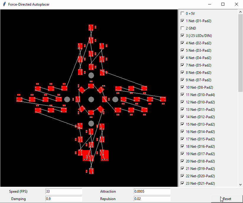
Using KiCad PCB parsing code I wrote for another project, I was quickly able to grab the nets and footprints out of a KiCad project. Displaying the nets and allowing specific ones to be turned off was a feature I identified as critical early on, because the ground or power nets would overwhelm any of the others, rendering the important nets useless.
Truthfully, a significant part of this was wrangling TKInter to build the Python GUI that I wanted. It was a success, but I’ve never used it before, and I am not a fantastic UI designer.
Under the hood, the system essentially treats each of the nets as a spring, and applies a simplified version of Hooke’s Law to each connection. Each of the centre point of the footprints acts as a charged particle, and a simplified version of Coulomb’s Law acts upon it to repulse all of the other footprints. These algorithms are a pretty typical way to do this, by essentially setting up a physics simulation. One tweak on this strategy that is unusual, is that the nets don’t act on the footprint origin. They act on the pad itself, which allows a torque to impart a rotation on the footprint.
I’ve gotten this project as far as “fun tech demo”, and it’ll likely fall dormant for a while in this state. At some point, I will build an appropriate PCB using this technology, because I love making unusual designs that are electrically fine.
The repo is here. Have at it.