A lot of the switch-mode power supplies I’ve built have relied on Skyworks Technologies controllers. This is because they are very cheap, and seem to go obsolete almost immediately after purchase.
This is a quick story of bringing up a new switch-mode circuit from a different manufacturer to test its viability in some battery-powered devices.
I’m using a Richtek RT6150A buck-boost controller.
For a 3.3V output, buck-boost topologies are necessary when the input is a LiPo battery. The ~3.0-4.2V safe voltages for charge and discharge are perfectly bracketing the 3.3V target in a way that is about as inconvenient as possible.
Other than cost, the reason that I selected this chip was that it seemed marketed towards this exact application. Battery technology is written in the advertising materials, and the datasheet shows this:
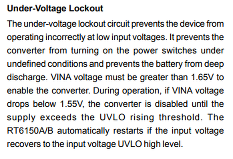
Oh yeah, perfect! An undervoltage cutoff. That should be good for LiPo protection.
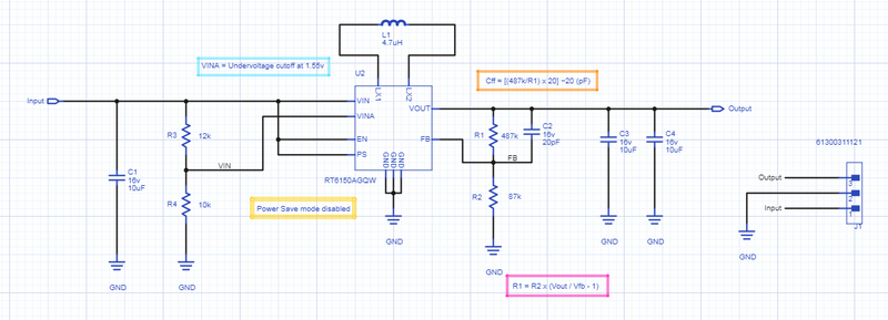
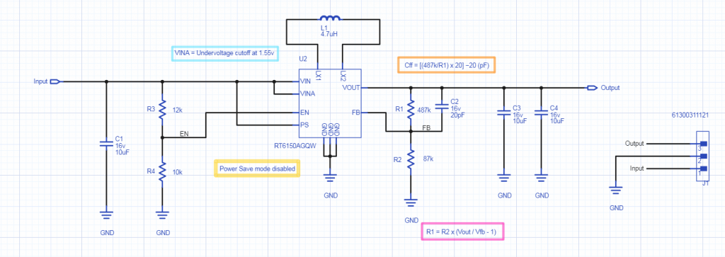
so I drew a schematic like this:
And then sent it off as a one-off PCB through OSHPark.
It costed about a dollar.
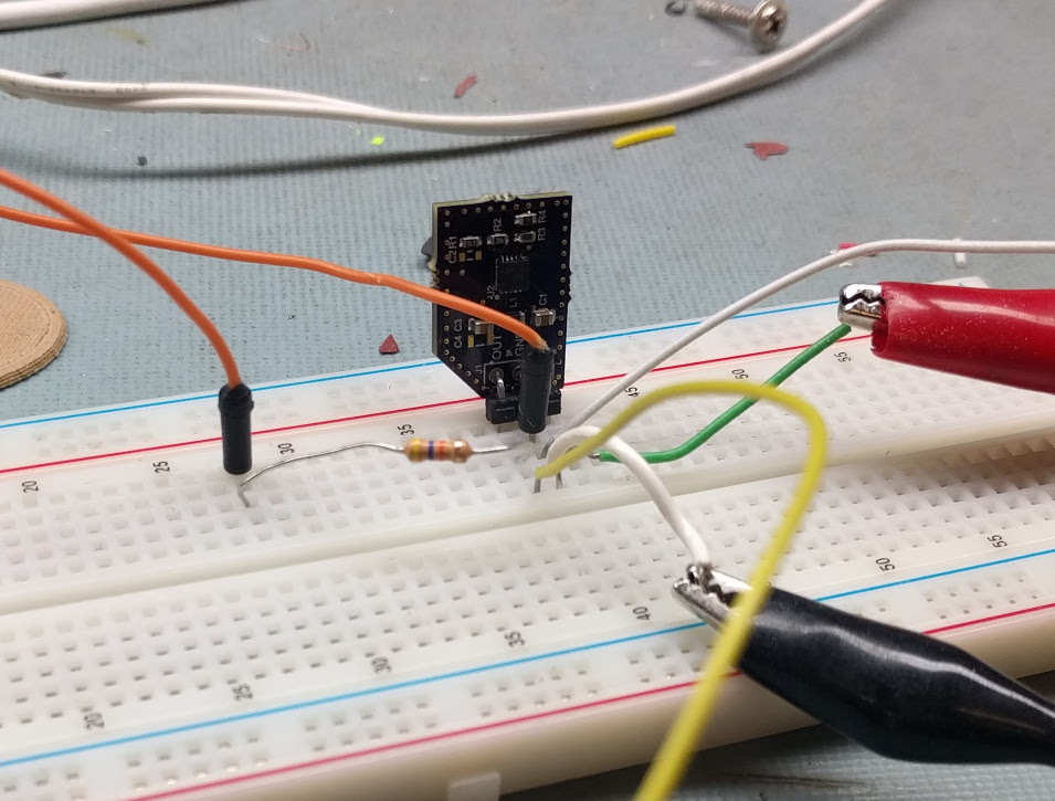
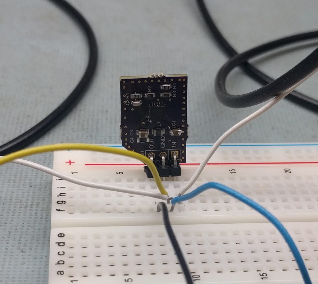
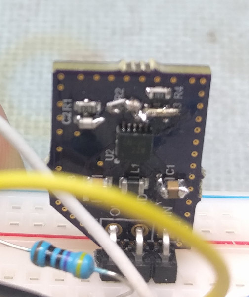
I got it back, soldered it, and did a quick bench-test. Instead of cutting off at 3.3v like I intend, it didn’t turn on until close to 5v.
No good!
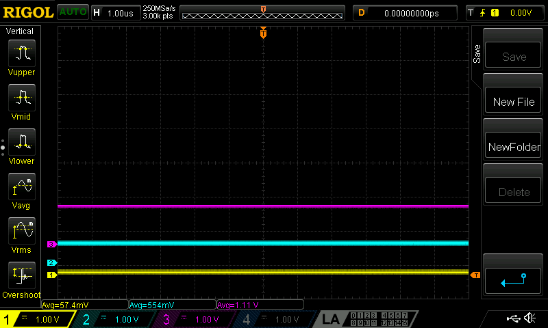
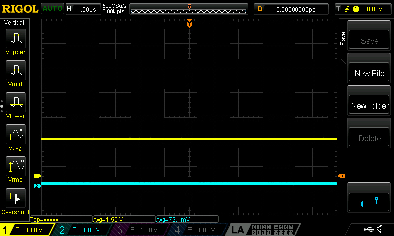
So I pulled out the scope and checked the voltage at VINA:
The input voltage was completely stable, so that wavy portion in the middle of the voltage divider wasn’t coming from the input.
Going back to the datasheet:

This was ambiguous, but hindsight tells me it’s not actually intended to be a voltage cutoff. This is just the power for the control circuitry itself.
What was happening was that the internal control circuitry was drawing enough current that the voltage at the middle of the divider sag enough that it hit its cutoff, and turned the chip off, making the voltage rise enough that it turned on again, etc.
This chip is advertised in Richtek’s appnotes as being good for LiPos because of that cutoff, I assumed, but it doesn’t actually work!
So, I bodged VINA to VIN, and now it works, albeit at the full range of the chip. That’s not exactly what I want.
The other thought is to use EN as the cutoff.
It’s supposed to shut the chip off at “logic level low” whatever that means for a wide input voltage chip.
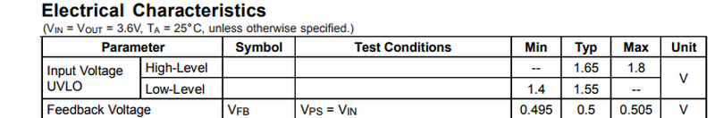
Logic level is anywhere from 1.4 to 1.8v, which is annoyingly wide.
But I gave it a shot.
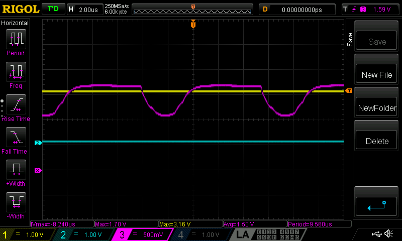
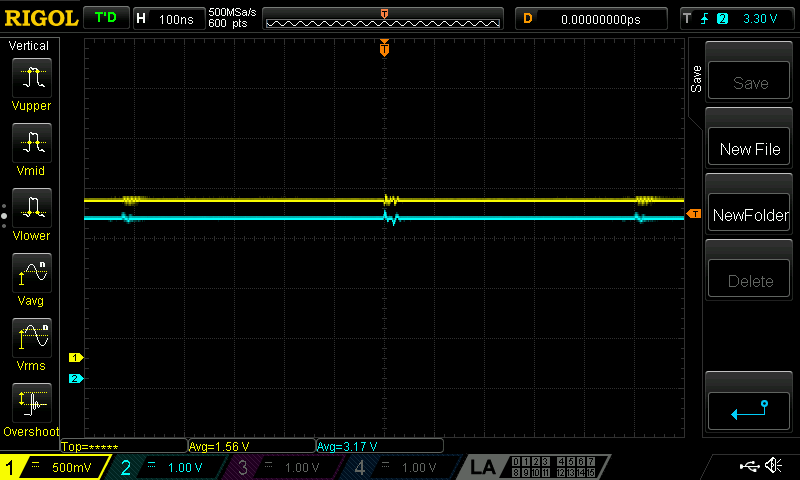
Some test results:
Channel 1(Yellow) is output, 2(Teal) is the EN pin, and 3(Purple) is the input voltage.
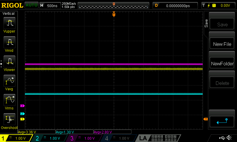
At 1.11V input, output is still disabled.
At around 1.59V, the output springs up to 3.24V:
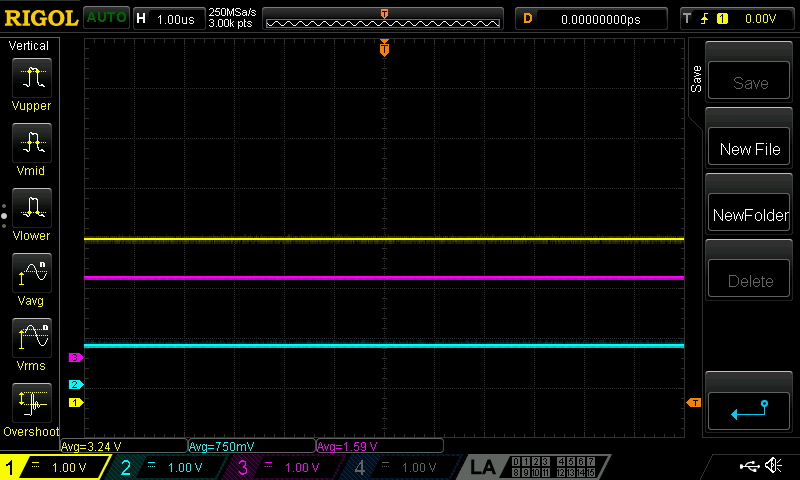
Weirdly, as the EN pin gets closer to the theoretically 1.55-ish point where it’s supposed to turn on, output noise starts to hugely increase:
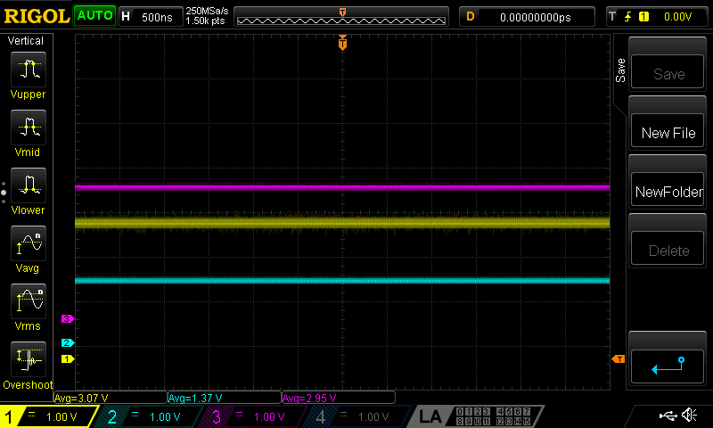
Until right at the logic level high point, the output voltage has almost a full volt of non-periodic, constant noise:
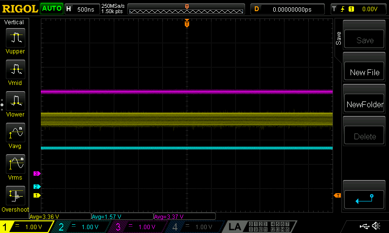
It’s possible that it’s not a coincidence that is right when the controller switches from boost mode to buck mode.
So again, let’s bodge this back into a manufacturer-recommended specification:
Replacing R3 with a 0-ohm resistor (or: a wire) gets this back into spec:
In this case, the output (teal) is still disabled until the input(yellow) starts to hit 1.50V.
From there, there’s a sudden switch-on at 1.56V to 3.2V output:
And it quickly rises to a 3.3V and stays there for the full range, up to 5V input:
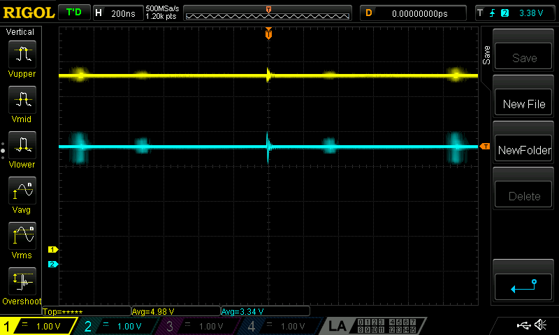
Output ringing is a periodic 1V peak-to-peak for about 20ns, every 1us or so. This gets a little lower when the output is loaded and provides some damping.
So the moral of the story is that the Richtek RT6150A works quite well, but only when the datasheet is closely adhered to. Anything “interesting” in the design leads to unacceptable noise or unpredictable results.
In the meantime, the RT6150A seems to be on the way to phasing out. Stock on Digikey is 0, with a 16 week lead time for new parts. The catalog not-so-subtly hints at using the RT6150B variant, and the datasheet is almost identical. The glaring differences are a few added lines in the marketing copy on the first page saying that fixed 3.3V operation is possible by tying the feedback pin directly to the output.
Anyway, that’s my debugging story. Nothing was particularly novel or unusual, but it was a good process to document irregularities while abusing the chip.
Pingback: I Made An IoT | In Which Jarrett Builds