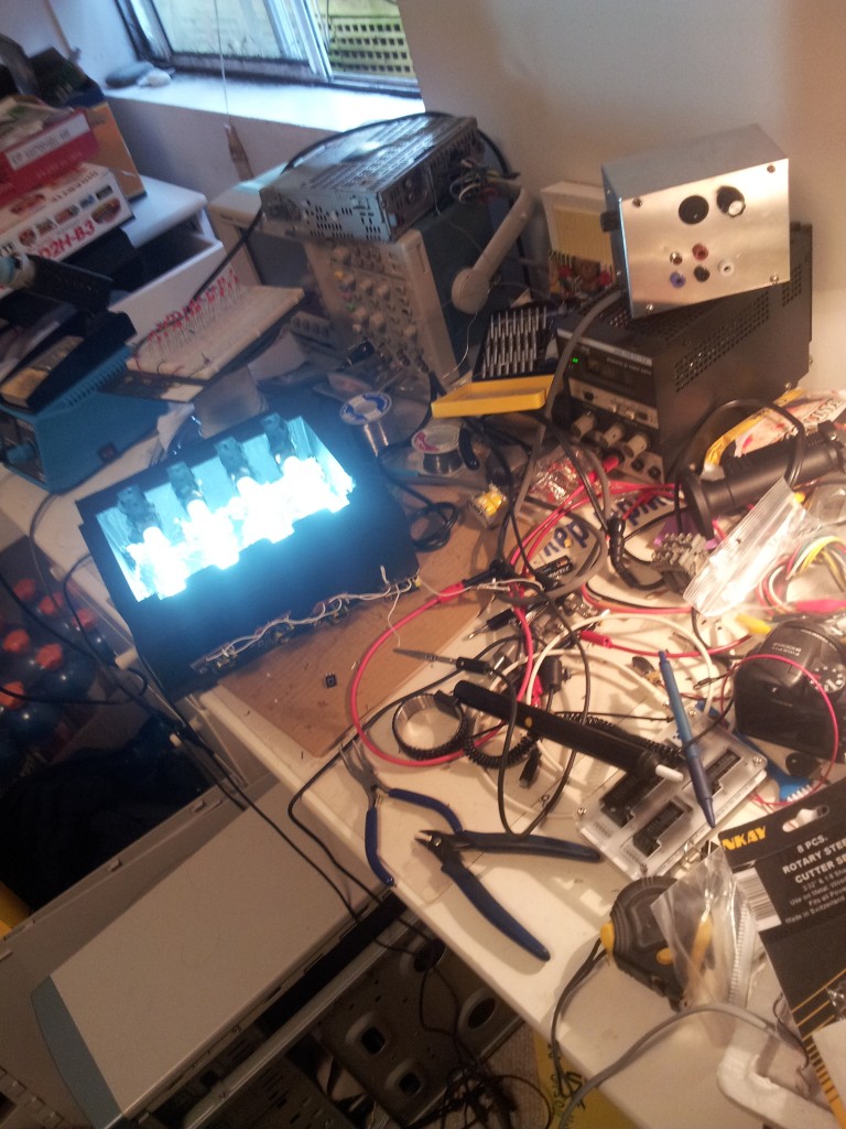
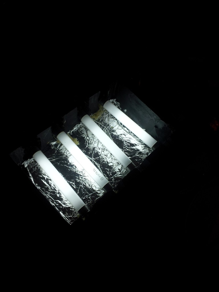
I should mention that sometime last year, I built a UV exposure box for manufacturing PCBs. It’s pretty rough, but I built it over the course of an evening to do one job, and it does it quite well. Or at least, I think it worked quite well.
The idea of being able to conceive of an idea, draw a schematic and PCB, and create a physical copy of the device in a single day is extremely attractive. The problem is that the exact method is not an exact science.
Sure, there are a set series of steps that must be taken – Design a PCB, print it out on a transparency and use it as a mask for a photosensitive coating on some copper-clad, set the coating, then etch off whatever wasn’t masked off.
But every setup is different. People on the internet are using a different brand of UV-sensitive copper clad (or coating it themselves), different suppliers for the chemicals, different UV lamps, etc.
I tried twice to etch my own PCB. The second time worked much better than the first, but I still need more tweaking with timings to get it right. After that (which took around an hour each), I realised that right now, with my job keeping my away from home most of the time, that my time is more valuable than the cost of sending out the designs.
So that’s been put on hold until I spend a significant time in town or get a new job. But it’s a pretty fun diversion, and a pretty useful thing to be able to do, so I’d like to come back to this.


