
Pickit is the officially supported programmer for Microchip’s PIC line of microcontrollers. The newest revision, Pickit 3, supports the latest and greatest micros, but does away with some fun stuff like in circuit debugging.
Fortunately, when Microchip dropped support of the Pickit 2, they open sourced the schematic so there are tons of clones out there that have all sorts of different features or design considerations.
There are through hole versions, dead-bug versions, versions built with components on hand, and versions built to original standards.
I’ll be using this Pickit 2 clone schematic:
http://diyfan.blogspot.ca/2013/06/original-pickit-2.html
I like this one because the official schematic has storage space for programming-on-the-go, which adds a lot of complexity. I have literally never used that functionality on mine, so I’d rather save the weight. All of these components are also easily sourced on the grey market. I’ve checked. They’re cheap.
Most clones are through-hole because they’re done on proto boards, but surface mount components are important here for keeping it low-profile.
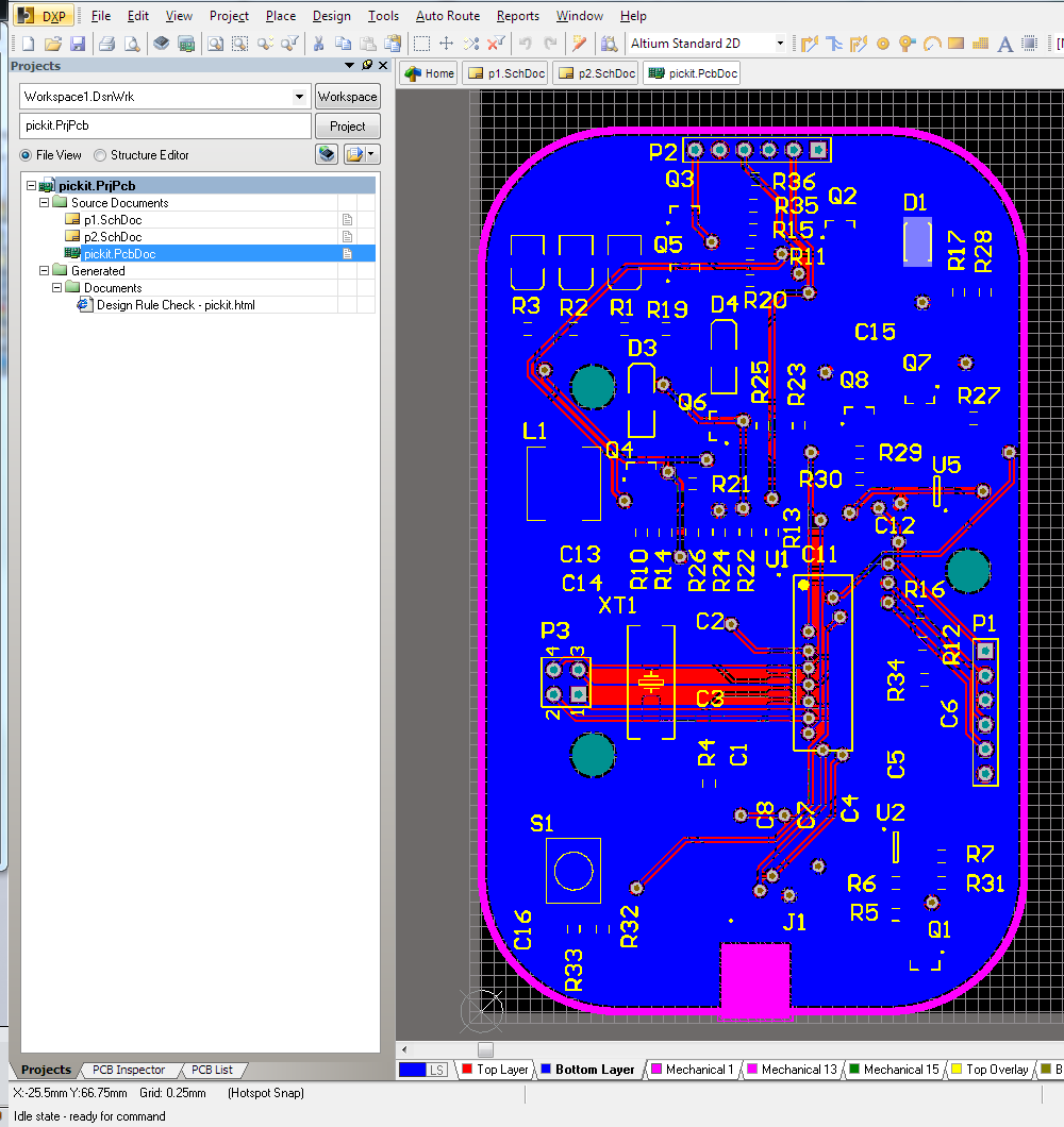
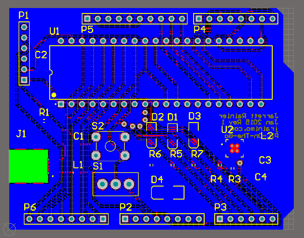
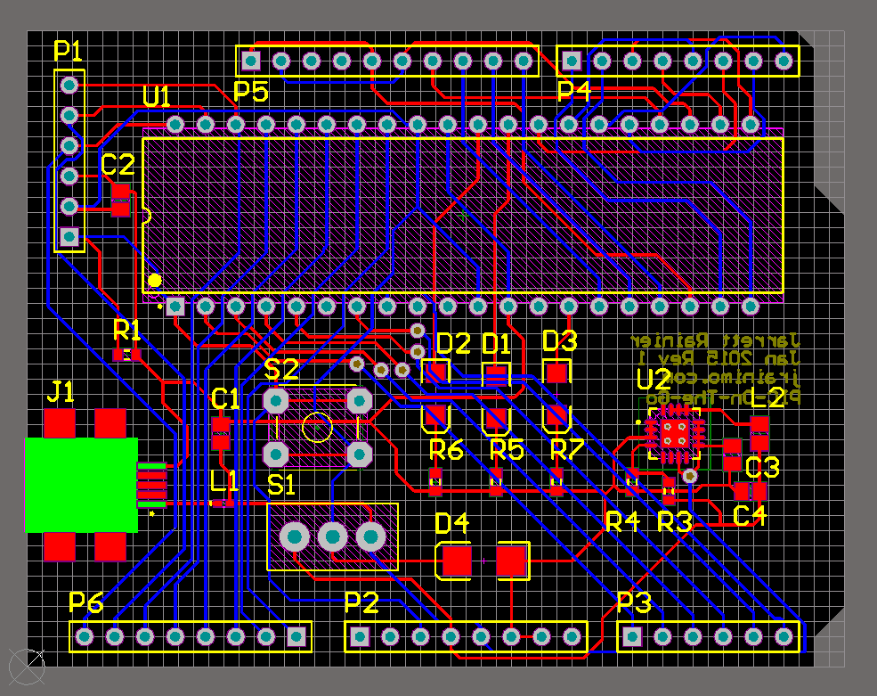
So I’ve redone it in Altium. I’ve add programming headers for the PIC itself and broken out all the spare pins, but otherwise kept it pretty close to the original schematic.
I’ve also decided to fit it in the gold standard of hacky enclosure styles: The Altoids tin.
It’s kind of surprising that I haven’t seen this done before.
Using the Altoids tin dimensions provided by Adafruit, I’ve designed this PCB. The tin will require some cut-outs, but it looks pretty simple.
Here’s a teaser:
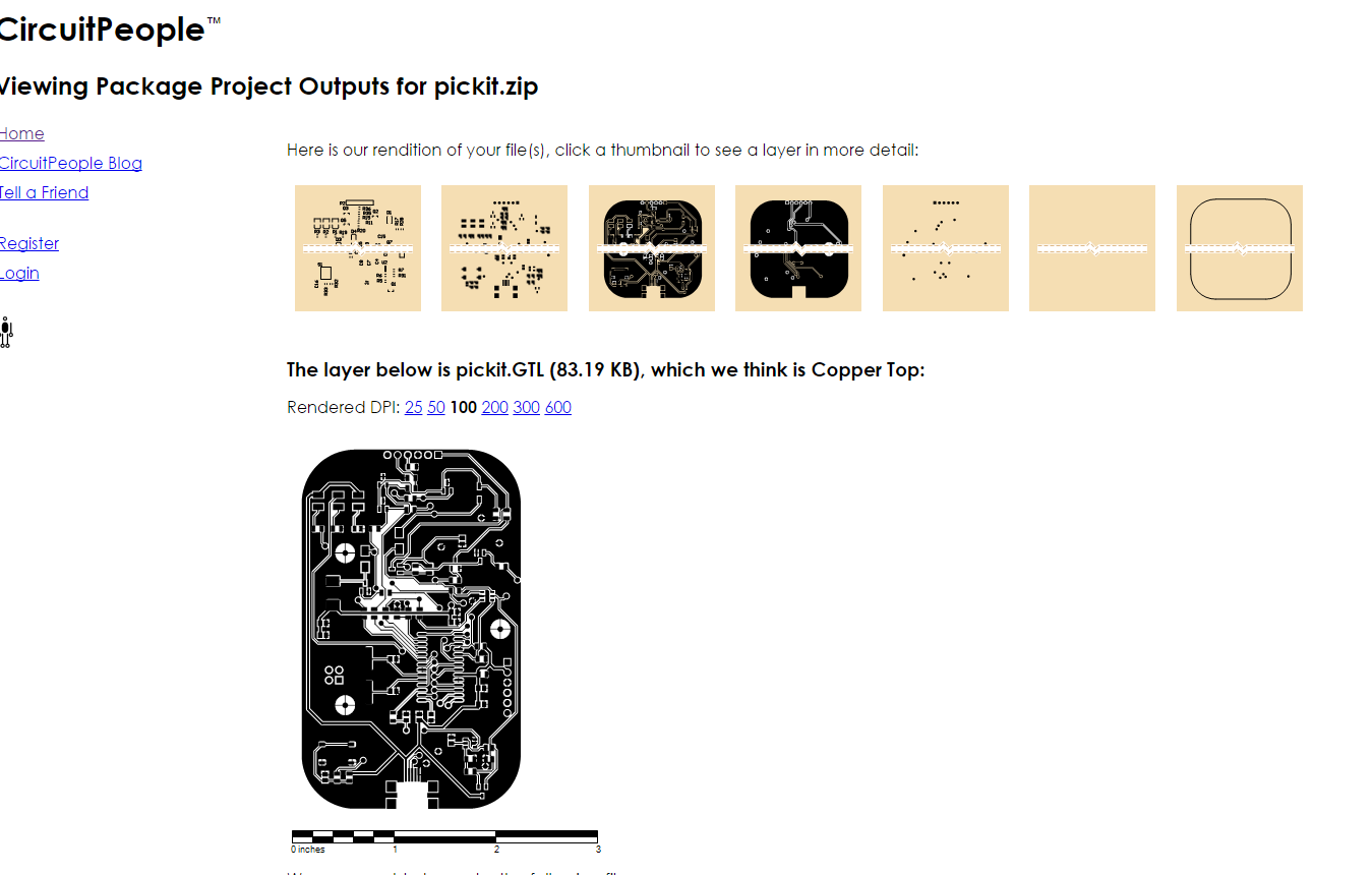
It’s two layers for cost, all components are on one side, and there are fiducial marks for a pick-n-place machine. Basically, I’m trying to make this manufacturable. I have no intention of doing so, but I did it because I could.
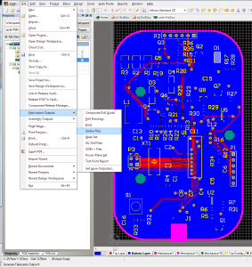
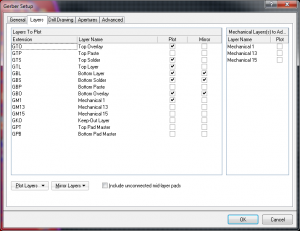
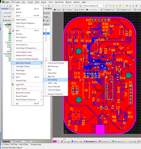
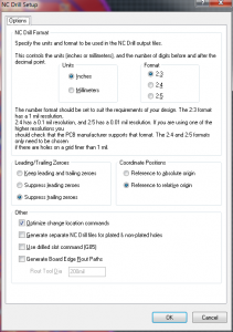
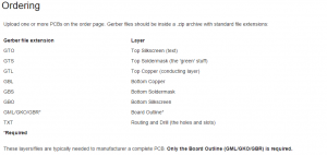
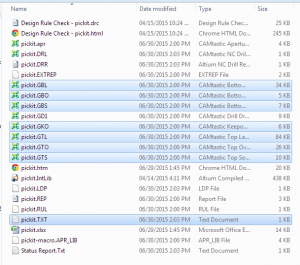
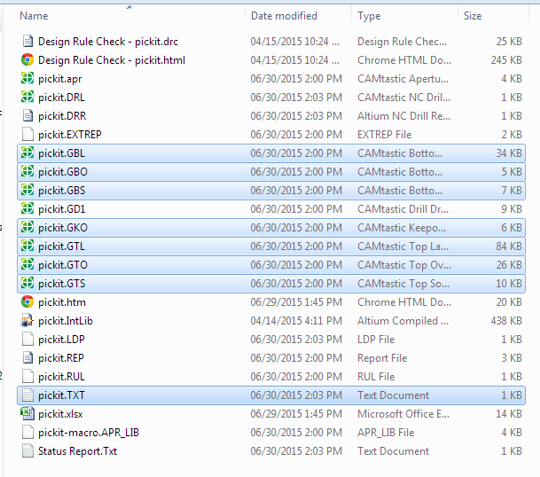
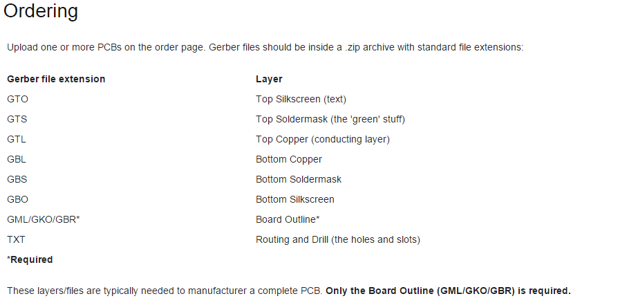
As usual for most of my projects lately, all files (including Gerbers) are here.
Note: The positive rail for the op amp is not connected to the VCC net. Whoops! Blue wire or respin required, if I ever come back to this.
