I’ve been a really big fan of PCBModE for a long time. Designing beautiful PCBs is a seriously difficult skill, and a serious abuse of the PCB board houses. Saar Drimer of Boldport has done a great job, and anyone reading this should definitely check out his stuff.
Where it falls down, though, is doing complicated and electrically correct circuits – No DRC/ERC rules, and not even a schematic view. I use Altium for my main PCB package, but it’s pretty tricky in it to get images into the PCB. It is possible, if a little convoluted, so here is my method.
Part of the problem is that I’m using Altium Designer 10 – Newer versions are better with this, it seems.
This process uses the CreateRegionsFromBitmap script. On my machine, it’s located in:
C:\Users\Public\Documents\Altium\AD 10\Examples\Scripts\Delphiscript Scripts\PCB\CreateRegionsFromBitmap
It’s also broken and required a couple fixes.
When I opened up PCBLogoCreator.PRJSCR in Altium and compiled/ran it, I got an error, missing semicolon at this line:
GrayWidth := Round((1 - sqrt(GrayProportion)) * PixelToCoordScale / 2);
Instead of trying to fix it (I don’t got time for that), it was replaced with:
GrayWidth :=0;
Second error was a missing function. This was fixed by copying LayerComboBox.pas from the PCB Logo Creator script into the working CreateRegionsFromBitmap script directory and project tree.
Then hit Run, and a dialog box pops up!
My workflow here was to identify what different shades I could get on the PCB, and the best ones for my image.
Here is a list of portions that contain wildly different shades:
- Bare FR4
- Copper
- Soldermask
- Soldermask with copper underneath
- Silkscreen
Predictably, that means that images with 5 or fewer colours (including backgrounds and outlines!) work best. For a non-commercial practice piece, Dr Seuss was the clear choice.
First step is to pull the desired image into Inkscape and separate all the component colours.
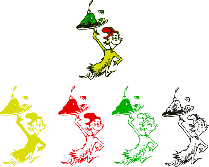
The way Inkscape handles colours masking each other – like the yellow layer being the “background” and relying on it being blocked by the colours on higher layers – doesn’t really mesh with the way they show up on PCBs. After some fudging around (as quickly as possible), this is what I came up with.
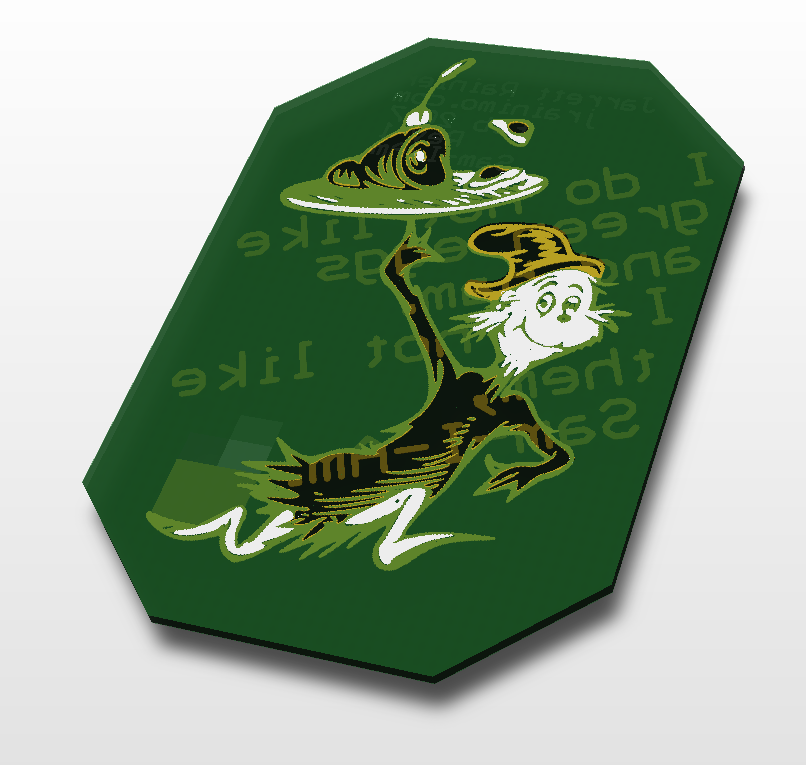
And here’s how the PCB turned out in OSHPark Purple.


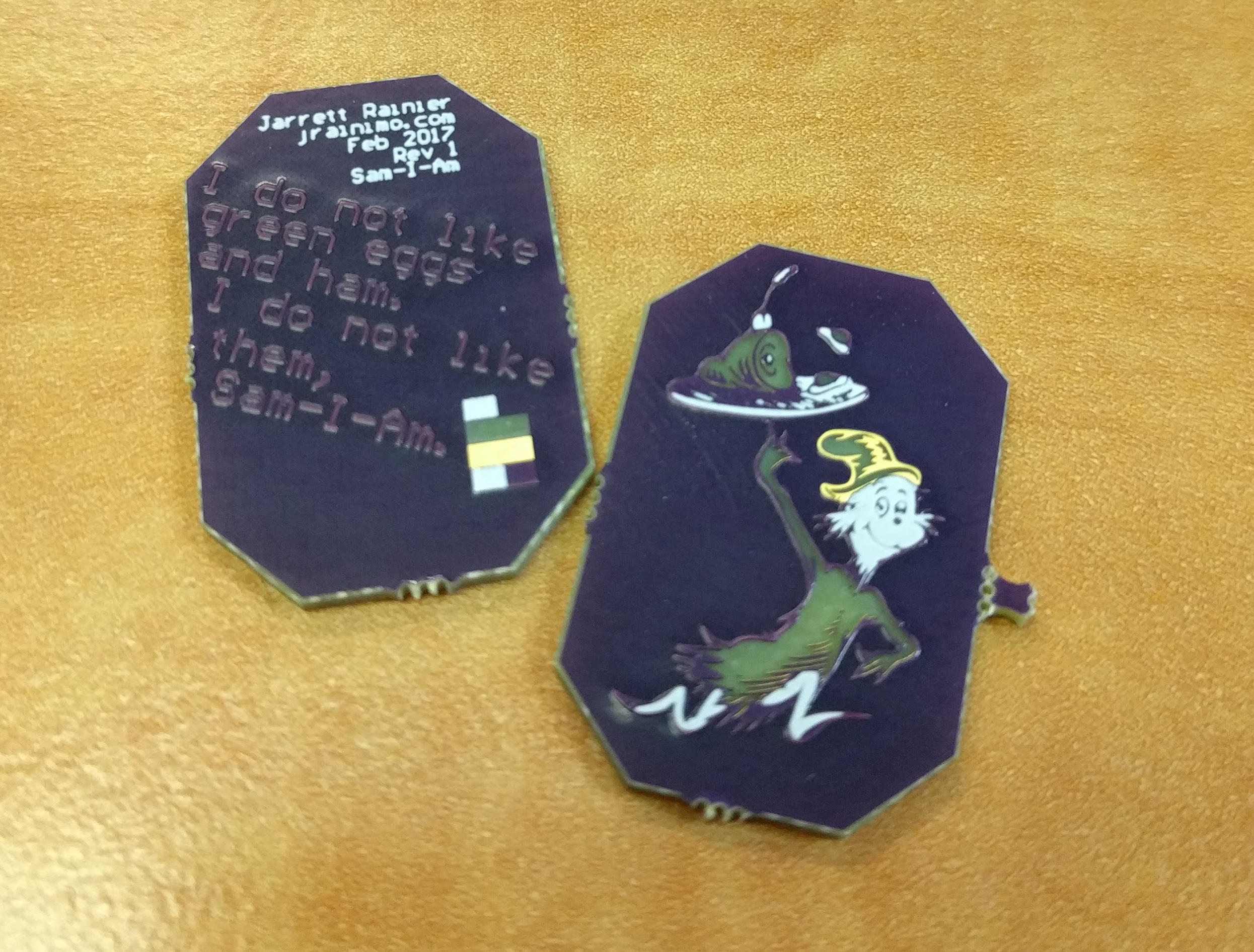
The thing is super small, so you can see how the soldermask pools up against the raised copper and causes weird bubbles.
I didn’t spend a huge amount of time trying to fit the best colour scheme to the image. But what I’ve done since then is scanned a few PCBs that I have kicking around, and created this handy palette for a various soldermasks!
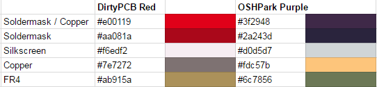
The best method for using these is probably to ignore the PCB aspect entirely at first, and draw a pretty picture in your illustration application of choice, using just those colours. Translating that to PCB is the secondary concern, and much easier. Something to note is that the “copper” colour of the DirtyPCBs palettes is HASL tin grey on top, and the OSHPark scheme is ENIG gold on top. Both of those are shiny.
Another technique worth trying is crosshatching. That might work out really well, in the same way that it works for laser cutting.
Pingback: Getting Images into CircuitMaker | In Which Jarrett Builds
Pingback: Sugar Glider Wifi Throwies | In Which Jarrett Builds
Pingback: An Extra Special Parcel from China | In Which Jarrett Builds