Archive for Jarrett

Rapidly Building Software to Prototype Quickly


TLDR: I wrote an Inkscape extension to make my life a little bit easier when designing assemblies with laser cutters.


For the most part, I avoid using 3D printers while rapidly prototyping. Until very recently, they have been little better than toys; unreliable, inaccurate, and high maintenance. The laser cutter, however, is a tool. By cutting and joining multiple sheets, three-dimensional objects are still faster and often better than 3D printed parts.

Additionally, when I’m trying to build something really fast, I find it much quicker to sketch out profiles in Inkscape than CAD them up. Inkscape is totally rad open-source vector drawing software, if you’re not familiar. Being able to see assemblies in 3D is nice, but I can do that in my head for quick and dirty projects.

One of the bottlenecks in this process that really messes up my flow is hand-drawing box joints. It’s tedious and error-prone to copy mating profiles that are dimensionally accurate.


But wouldn’t it be great if it only took two seconds?

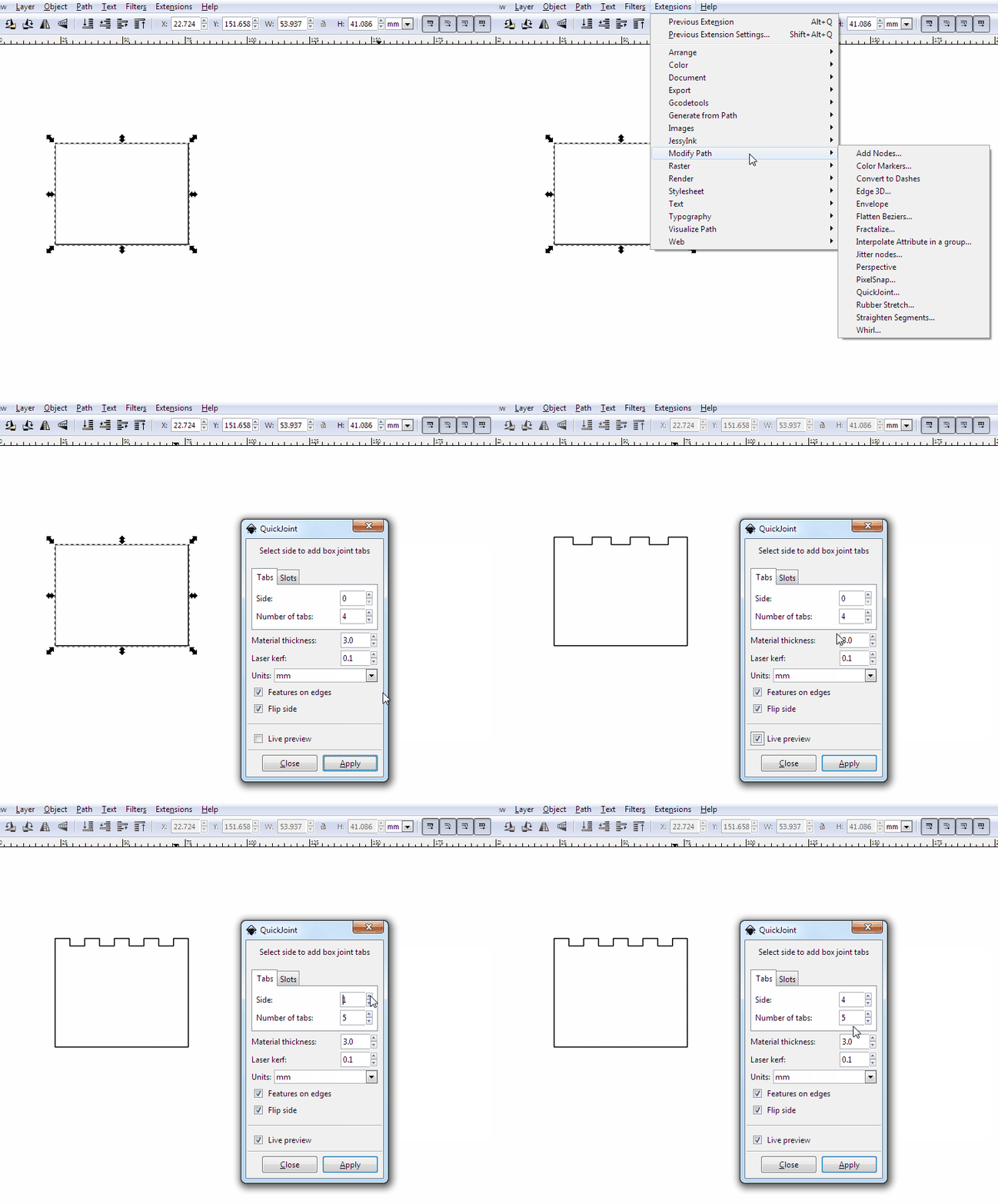
So this is QuickJoint. It’s a simple Inkscape extension that will add box joints to selected objects.


This first version can do male tabs or female slots. The tabs by selecting a path, and then in the menu choose which side (and direction) to tabify.

The slots will use a single line as a guide, accounting for the laser’s kerf.


This is a work in progress. Fine tuning with how kerf computation works will be tweaked. Slots/tabs may be changed to autodetect so that everything can be done at once. There are a few more changes, for sure.


It’s been tested on Inkscape 0.91 and 0.92, but there was a breaking change in how units are translated in earlier versions, so if you get an error that references self.unittouu, then upgrade your copy of Inkscape! Feel free to submit other issues, with example SVGs.


For a two-minute primer on writing extensions for Inkscape, read on!

Everything is based out of the Inkscape/share/extensions folder.

The recommended method to get started is to find a similar extension to the final project, and use it as a starting point.

Two files are required: A .py and a .inx

The .inx is an Inkscape extension dialog file. There’s a reference here, but for simple stuff, that’s not needed. There are plenty of decent examples in the extensions folder. You’ll start by modifying the dialog options, and then setting the self.OptionParser.add_option of the Python script to match.

For the Python portion, there is a little bit of magic.

Most of the files in the extensions folders are just that: extensions. A few of the files in that folder are special helper files, though. They’re listed here. Inkex has the main Inkscape helper functions, and I used simplepath for SVG writing.

One of the key concepts is that Inkscape mostly gets out of your way while running the Python script. You’re parsing and handling the SVG files directly, with the assistance of those helper scripts. It’s not so bad, SVG is a really simple format – In this case, I only needed commands relating to straight lines, listed full SVG spec.

When Inkscape calls your function, it runs YourExtensionClass.affect(), inherited from the Inkex module, which then calls YourExtensionClass.effect(). Yeah, not a typo. It’s a little bit silly.

From there, the “Live Preview” checkbox in the extension dialog is your friend. The .inx only gets loaded when Inkscape starts, so changes to the dialogs don’t get updated, but the .py gets re-run every time the extension renders.

Sugar Glider Wifi Throwies


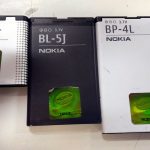
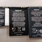
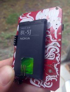
I have access to a big box of Nokia phone batteries. This is a problem. It is very large. I do not have enough Nokia phones to use them all.

There are three sizes:

BP-6MT (1050mAh), BL-5J (1320mAh), and BP-4L (1500mAh).

After some catalog-hunting (be vewwy vewwy quiet), I’ve found the connector they use, the A117827CT-ND.


Update: This handy website has sizes of various batteries listed.


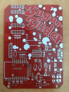
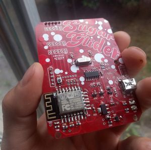
This PCB – I call it “Sugar Glider” – is a battery-powered ESP8266 wifi module. It supports charging a single LiPoly/Li-Ion battery over USB, running off the battery, or both while it’s plugged into your choice of MicroUSB or Mini USB connector.

Mostly using the reference design of the MCP73831 charger chip, and it powers an ESP8266. There is also a CH340G USB-serial chip for programming, so it basically acts like a NodeMCU.


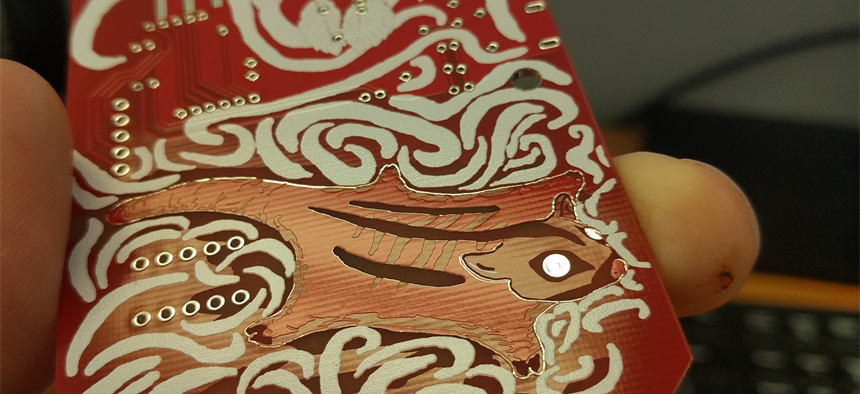
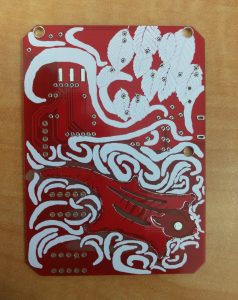
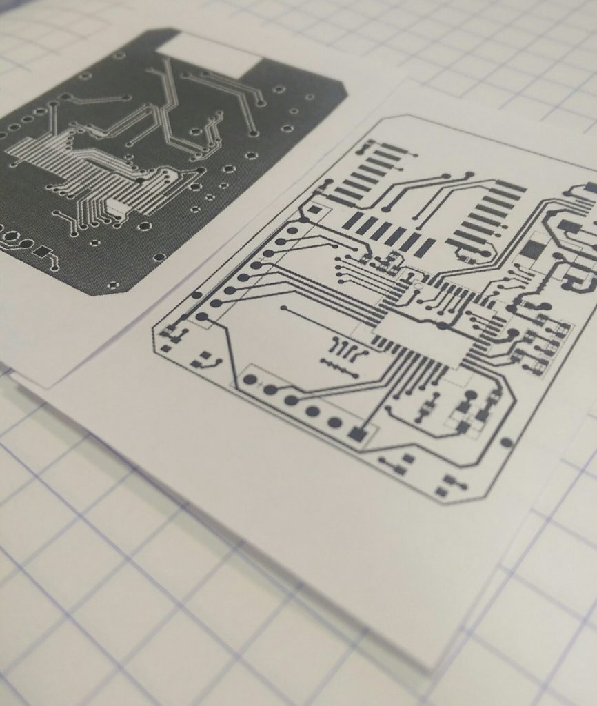
But wait, there’s more! Despite the simplicity of the design, and really not caring that much about it, it took a tonne of time. That’s because I’m rusty at drawing from not having done any in the last decade, and it looks like this!


This was done by exporting gerbers, converting each layer to B&W images, then loading them up in my (also decade old) copy of Photoshop. They were coloured according to my sampled colour palette, and then drawing commenced.

When I was done, they were loaded back into CircuitMaker using the techniques detailed here and here. I think I’ll try to do more of this in the future. Having this much unused PCB space is rare, though – It was needed to act as a sled for the batteries, so it’s quite large. Usually I make boards as small as reasonably possible to save on costs.


The assembly went reasonably smoothly. You have a choice of populating the micro- or mini-USB connections. I prefer the mini, because there are something like 20 different possible microUSB connector footprints. In future versions, I’ll probably also use a 0-ohm resistor to select which one. Having an unpopulated connector on the same line is a recipe for bad signal integrity and unwanted antennas.

The power supply portion of this is simply a low-drop out (LDO) linear regulator, because I wanted to bang this circuit out quickly without having to design a switch-mode power supply (or: the Right way to do this project). Slight problem: the LDOs I sourced from China, well, weren’t very LDO. They had a full volt drop across them, leading to 2.7v seen on the ESP8266 at nominal battery voltage. No bueno.


The solution is very simple; just replace the regulator with a proper part from Digikey, that comes with a datasheet. Modern ones are usually closer to 0.2v. That’s the stuff.

This project was created in CircuitMaker. Here’s a link the cloud project page, but here is a zip file of all the relevant files – Schematics, PCBs, gerbers, and layer drawings. The resource-heavy images don’t play nicely with PCB design, so I recommend deleting them while editing the PCB, and then adding them back in right before export.

Getting Images into CircuitMaker

Jumping off from my last post about getting images into Altium Designer, it was surprisingly difficult to do in CircuitMaker.

After three days of attempting a few different approaches, I have one that I’m quite happy with. Conveniently, this is pretty good at getting images into EAGLE as well. At least as good as the built-in ULP.

If you’re just here for the solution, scroll way down and read the paragraph about the brd-builder.py script.


This is the story of how I arrived at a robust method of importing bitmaps into arbitrary layers in EAGLE cad or Altium CircuitMaker.


The first approach I started with, after drawing some pretty pretty pictures, was to attempt to load them into Altium Designer in the same fashion as described earlier.

These images were way larger and more complicated than the previous experiment, however, and the Delphiscript chewed on it for three or four hours before silently failing. Even if it had worked properly, I’m not particularly happy about being dependent on the expensive professional tool to work with the hobbyist one. So I delved deeper.

Here are the options and approaches I took:

  • Importing DXF files directly in Circuitmaker is possible, but largely unsatisfying. The CM importer splits up the original paths into discrete arc and line segments. This is great if you want to draw outlines, but that’s it. Lack of fill options or the ability to merge these objects make it inadequate for my purposes.


  • Using CircuitMaker “region” objects. Going into the property menus of one of these objects reveals a list of points and coordinates, and import/export options. I wrote a converter to massage SVG files into the proper CSV format. This is svg-parse.py. It’ll take an SVG file, and convert each individual object into a CircuitMaker-compatible CSV file. From there, you can create a region in CircuitMaker, open its properties, and import one of the CSV files.

This is pretty good, and results in native objects that are speedy to move around. There are some caveats, however:

  • You must do this for each object, making it labour-intensive for complex canvases
  • Curves are not supported, so it is first necessary to follow the “Add Nodes” and “Flatten Beziers” steps in Inkscape, described in the import-dxf EAGLE plugin.


  • Attempting to hijack the clipboard was the next experiment, read-clipboard.py. Region objects can be copy-and-pasted between documents, so I wanted to take a look at what that data contained, and maybe silently insert my own. This never really worked properly, and I abandoned it quite quickly. It was a hacky approach, anyway.


  • A quick search on reverse-engineering Altium’s file format brought up this primer (by way of Hack-A-Day). Although very abbreviated (the goal of that guide is to teach a methodology, not to completely reverse the file format), the page was more than enough information for me to write a Python script that opens and dumps the contents of the CircuitMaker-formatted OLE document. So in ole-extract.py, I got as far as grabbing a library document and extracting and splitting header/data information into a folder. Realised at this point that the libraries I was using would have a difficult time repacking the streams into one OLE document. Not to say it isn’t possible – it totally is – it’s just rabbit-hole I don’t particularly want to go down at this time. This is still interesting in that it should be a working Altium and CircuitMaker file reverse engineering effort in Python, which hasn’t been done before.


  • Importing EAGLE files works really well. They’re XML-based, and very well documented. First, I imported an EAGLE file that contained an image, which looked and worked great in CircuitMaker. I poked around with how that image was created in EAGLE, and it looks like it was just made with the built-in “Import Bitmap” ULP. How it works is that it scans along each horizontal line, creating a one-pixel-high rectangle in the filled area. Repeat for the entire image.

Okay cool. That sounds really simple. Problems with that:

  • It doesn’t alleviate my allergy to using 3rd-party software as an intermediate step
  • If my image is over the 3 inch (or whatever) size limits of EAGLE’s free version, I’m hooped
  • The ULP script seems to choke on images randomly

So what I did instead, is take a dummy EAGLE file, and stripped it to the bare-necessities required to load. This particular brand of XML is the fourth file format I’ve had to parse in this whole process, but it wasn’t too hard. With this dummy file, my final and greatest script, brd-builder.py, grabs a bitmap file, converts and then injects it directly into the EAGLE file, giving you a proper EAGLE file, with no size limitations and no EAGLE install required. CircuitMaker can then easily import this via the File->Import menu.

Input images need to be a 1-bit BMP file.  In Photoshop this is done by converting to grayscale in Image->Mode->Greyscale and then converting to bitmap in Image->Mode->Bitmap. In GIMP, this is done through the menu in Image->Mode->Indexed. Then save as BMP.

Before running this script, open it up and then modify the desired variables – inFile, outFile, layer, and scale. They should be fairly self-explanatory. Scale in my application was found by guessing until it fit my board, due to the resolution I drew my image at.


This was a fun detour. Fun is good, because spending time to make tools for your tools can be very frustrating. The last tool in particular works great for me, but If I were to develop a robust system designed for anyone to use, there are a few more avenues I would attempt to pursue first:

  • In the Hack-A-Day link posted above, one of the comments mention being able to just open OLE. They turned out to be using 7zip, which supports that format natively. Coincidentally, I found a portable 7zip executable in the CircuitMaker folder. It’s possible that they’re using this for encoding their documents. It would be fun to write an executable shim with the same filename that invisibly passes arguments to the original 7zip program, but logs it to file as well. Will also look into better methods for doing this – Static analysis using X64_DBG or IDA is an obvious candidate here.


  • Failing that, writing and testing code to modify the OLE document stream and then repack it into a format that CircuitMaker can read


  • The native importers in the CircuitMaker all have IWZ extensions, and from the binary data seem to be x86/64 executables. Google says these might be installer files. Along the same lines as the executable shim/wrapper above, figuring out how these work and writing my own would be fun.

Cosmetic Surgery on Altium Boards

I’ve been a really big fan of PCBModE for a long time. Designing beautiful PCBs is a seriously difficult skill, and a serious abuse of the PCB board houses. Saar Drimer of Boldport has done a great job, and anyone reading this should definitely check out his stuff.


Where it falls down, though, is doing complicated and electrically correct circuits – No DRC/ERC rules, and not even a schematic view. I use Altium for my main PCB package, but it’s pretty tricky in it to get images into the PCB. It is possible, if a little convoluted, so here is my method.


Part of the problem is that I’m using Altium Designer 10 – Newer versions are better with this, it seems.


This process uses the CreateRegionsFromBitmap script. On my machine, it’s located in:

C:\Users\Public\Documents\Altium\AD 10\Examples\Scripts\Delphiscript Scripts\PCB\CreateRegionsFromBitmap

It’s also broken and required a couple fixes.

When I opened up PCBLogoCreator.PRJSCR in Altium and compiled/ran it, I got an error, missing semicolon at this line:

GrayWidth := Round((1 - sqrt(GrayProportion)) * PixelToCoordScale / 2);


Instead of trying to fix it (I don’t got time for that), it was replaced with:

GrayWidth :=0;


Second error was a missing function. This was fixed by copying LayerComboBox.pas from the PCB Logo Creator script into the working CreateRegionsFromBitmap script directory and project tree.

Then hit Run, and a dialog box pops up!


My workflow here was to identify what different shades I could get on the PCB, and the best ones for my image.


Here is a list of portions that contain wildly different shades:

  • Bare FR4
  • Copper
  • Soldermask
  • Soldermask with copper underneath
  • Silkscreen


Predictably, that means that images with 5 or fewer colours (including backgrounds and outlines!) work best. For a non-commercial practice piece, Dr Seuss was the clear choice.

First step is to pull the desired image into Inkscape and separate all the component colours.

The way Inkscape handles colours masking each other – like the yellow layer being the “background” and relying on it being blocked by the colours on higher layers – doesn’t really mesh with the way they show up on PCBs. After some fudging around (as quickly as possible), this is what I came up with.


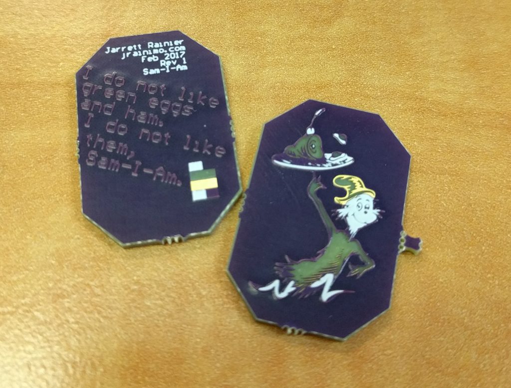
And here’s how the PCB turned out in OSHPark Purple.


The thing is super small, so you can see how the soldermask pools up against the raised copper and causes weird bubbles.

I didn’t spend a huge amount of time trying to fit the best colour scheme to the image. But what I’ve done since then is scanned a few PCBs that I have kicking around, and created this handy palette for a various soldermasks!

The best method for using these is probably to ignore the PCB aspect entirely at first, and draw a pretty picture in your illustration application of choice, using just those colours. Translating that to PCB is the secondary concern, and much easier. Something to note is that the “copper” colour of the DirtyPCBs palettes is HASL tin grey on top, and the OSHPark scheme is ENIG gold on top. Both of those are shiny.

Another technique worth trying is crosshatching. That might work out really well, in the same way that it works for laser cutting.

Anatomy of a Pen

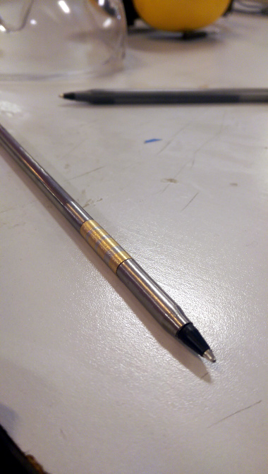
I’ve written recently about machining my own custom pen because, much like lamps, they are a “form over function” project where the end result can be gorgeous as well as useful. Aesthetically pleasing to everyone, not just techie people. And they don’t take up a lot of space!


Initially, my design for the first pen was sketched out in notebooks, and then modelled in CAD, then back to the notebooks when I was in the shop. This helped me get a general feel for what I wanted, but many style, material, and mechanical considerations had to be redesigned on the fly as I found techniques that didn’t work, and others that did.

A lot of the dimensions of final product came down to how they felt in my hands, as I was building. That’s fine for a one-off, but I’d kinda like to parameterize basic measurements so that I have some guidelines on what works for future pens.


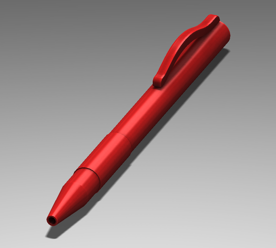
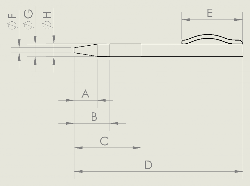
So here’s a pretty generic pen, modeled in Solidworks.


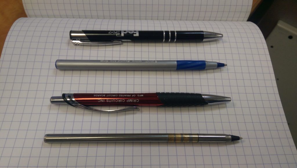
Here are a few pens I had within arm’s reach.


Starting at the top, I named these 1-4, and made some basic measurements based on the generic model:


Now I’ve got a good baseline for what makes a comfortable writing utensil, a recommendation for critical dimensions to stay within, and some language (or at least letters) to be able to intelligently discuss the anatomy of a pen.

Sure, we’re brute-forcing, but what’s the rush?

Ironically, in the process of writing a really fast implementation of the WPA2 encryption scheme, it was necessary (or at least easier) to first write a really slow implementation.

Here is my wpa2slow Python module.

To be fair, the actual speed at which this hashes isn’t the point. The point is that I have an entirely native Python implementation of how the entire WPA2 algorithm works, with an emphasis on code being clean, easy to read, and forgoing any speed optimisations that hinder legibility. Judging from the quantity of misinformation I’ve seen while researching this topic, someone will find this project useful. A lot of people have been having trouble trying to fit all the pieces together, over the years.

At first, I included the pieces as mock objects for unit testing. Each of the pieces (SHA1, HMAC, PBKDF2, etc) were built up over a period of several months, vaguely mimicking the interface format of equivalent existing hashlib libraries. Unfortunately, all of the standard Python hash libraries are really inconsistent!

For example, to hash a string with SHA1, I’d use:

output = hashlib.sha1(str)

Makes sense. But to then hash it with HMAC-SHA1, I’d do:

output = hmac.new(secret, value, hashlib.sha1)

Which is pretty weird, in this context. It makes more sense when you realise that HMAC can work with multiple sub-algorithms (commonly SHA1 or MD5), and you can go multiple rounds with adding more salt. That’s not the case in my implementation, however, so copying the format was a mistake.

One thing that rests solely on my shoulders is the massive amount of debugging information, hacky fixes, and generally poor code I’d written while focusing on an entirely different problem.

If I had written it cleanly from the beginning, it would have been a lot less work, that was silly of me.


Anyway. It’s pretty decent now. Check it out, read the docs, or install it!

pip install wpa2slow

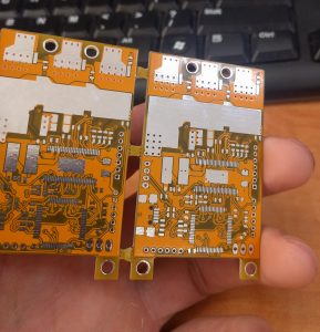
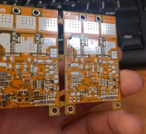
ReacTick R1.5

Prototyping aw yeah.


After the first version of my LCD widgets, there were some things that I was planning on changing for the next respin. R1 just to get some hardware in my hands and start writing code. This next one is all about the cleanup.


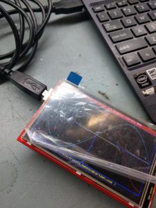
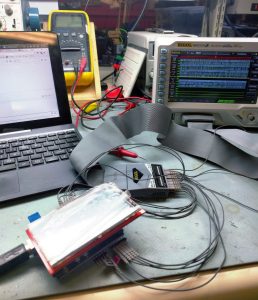
The last version of R1 is here on GitHub. It works… Poorly. The code in the test folder is stuff to help me prototype, before I got to a working model. Originally, I tried writing an LCD driver in Python for the Raspberry Pi GPIO, but the output seemed super unreliable. Instead of taking the time to troubleshoot why, it was faster to port that code onto a PIC dev board, which worked great.

Once I had a known-good LCD (using the shift register), I finished soldering up the rest of the board and tried to bring up the whole board. It never quite worked properly, and here’s why!

When I was first drawing my schematic, the most common ESP8266 module was the ESP-12. Right around that time, November of 2015, the ESP-12E had just come out, with a bunch of extra pins. No one knew much about this at the time, but the conventional wisdom suggested that it was safe to include them in my design, allowing me to get away without using an additional microcontroller. Turns out these extra pins are associated with the flash memory, and using them willy nilly causes strange reset issues. Guess what kept happening when I was trying to test my fully populated board?

So before a complete rethink was in the cards, here was the original plan for revision 2:

  • The LCD has two little mounting tabs on the sides. An appropriately sized via to accommodate them will make the LCD fit better and prevent wobble
  • One of those mounting holes will interfere with the switches. Move them somewhere else. Specifically on one of the short edges, because the current location causes damage to the LCD when the buttons are pressed while the screen is face down on a table
  • Silkscreen for momentary switches to include functions (RST / PROG)
  • Add in the clever circuit that the NodeMCU group uses to enable button-less programming
  • Remove all unnecessary resistors:
    • R7 connected to LCD_RST
    • R10 connected to LCD_RS
  • Change LEDs to 0805 or something similar. I’m using 3528s, and they are huge and super bright and look out-of-place
  • Change user-settable LED to connect to a pin that is not GPIO16. Apparently some manufacturers (not mine) connect it internally to the ESP8266 reset pin
  • Change all the SIPO shift register pins from bit-banging to use the ESP serial ports – Should be faster, and allows me to…
  • Change requirements from an ESP-12E module to just and ESP-12, which has fewer pins
  • Break out extra ESP pins to some unpopulated pads for future hacking
  • Break out LCD touchscreen pins for future hacking
  • Add more testpoints for debugging (and future hacking)
  • Big decoupling cap


Some of these ended up making it in, but the new system design deprecated other points. So what’s new in R2? Stay tuned to find out!

R2 Paper

A Quick Re-Intro to the Lathe

As my current favourite project is primarily a software one, I really need something on the side to keep my hands busy.


So I opted to do a small, easy metal lathe project. You know how those go, right?

It ended up taking over 40 hours, mostly because I am bad at this. But I learned a lot!


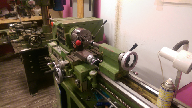
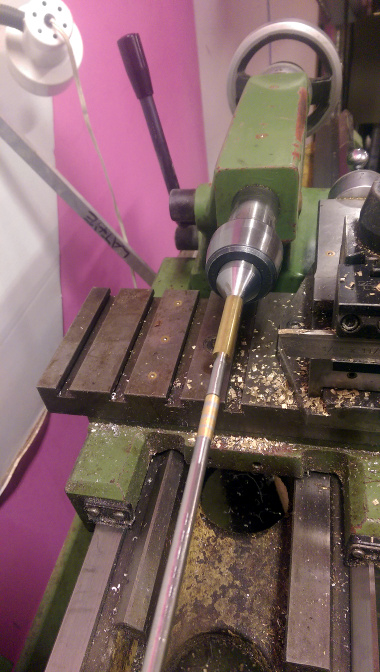
Here is the excellent old-school lathe I used:

pen1

Initially, this was going to be all brass, but Metal Supermarket doesn’t really carry a lot of red metals. Metal Supermarket is awesome, but pretty much the only stuff they carry is solid brass rod. It’s difficult to get a concentric hole through the entire length required by a pen, so that doesn’t work too well.

While browsing their stock, though, I found some gorgeous thick-walled stainless steel tube stock. Had to buy it.


I started out without a complete plan of what I was trying to do, and it’s clear that I was just playing around with shapes.

pen2

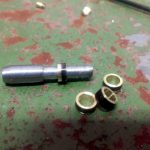
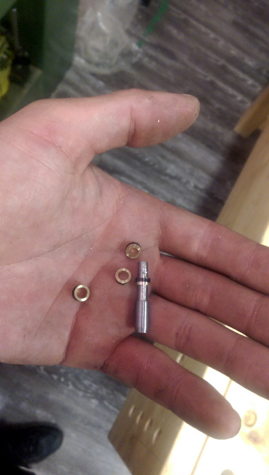
So I decided I liked that, parted off the left side, and machined some brass rings to go around the grip as extra bling.

You can see the scales I was working at, this all ended up being pretty precise work. Our lathe is a little large to comfortably get in to close features with the tailstock in use, but it’s still possible when you’re careful.

pen5

This piece had no way to effectively join it to the other side of the pen due to lack of forethought, so it had to be scrapped.

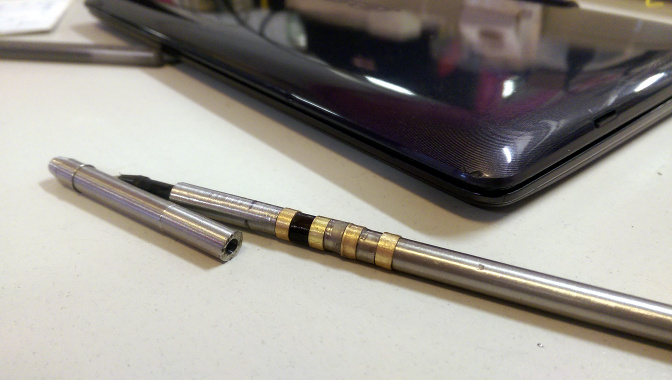
The next version was a little bit better, and shows the steel-brass-steel ring pattern, and kinda how everything fits together.

But then, one of the biggest takeaways I learned on this project is that working with stainless steel suuuuuuucks.

pen9

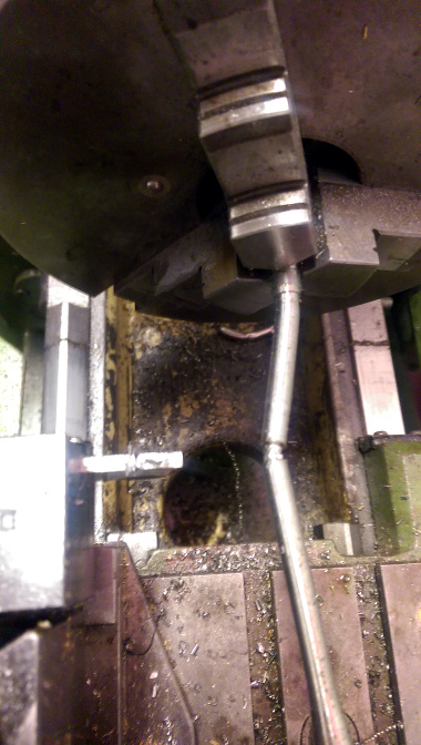
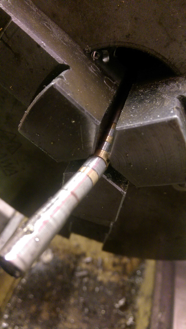
It’s really malleable, and is able to bend with low forces, even less than an inch away from where it’s being held.

Due to the high carbon content, it’s super hard on the tools and required frequent resharpening. When the tools are dull, the metal goes straw-coloured due to heat treating really quickly, and gets even harder.

So here’s attempt number three. I’m at about thirty hours by now, but getting faster after every failure.

pen10

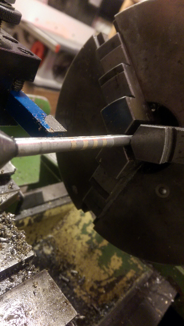
I’ve attempted to fix everything together with superglue for machining, but there are issues with that. I’ve seen people use superglue for all sorts of workpiece holding in brass, but brass is really soft and easy to work with. While trying it with steel, the forces are much greater, in addition to the steel getting warm and melting the glue. Basically an exercise in frustration and not really worth it (for steel).

Nevertheless, regluing often and working slowly eventually starts to get results.


pen11


Until…

pen12

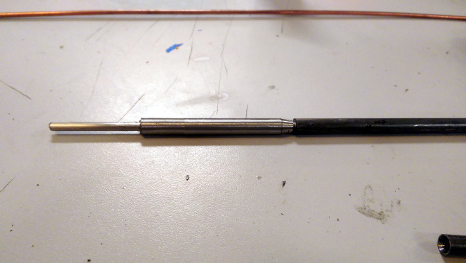
Attempt number four used a separate aluminum piece that I machined into a very thin-walled tube – about one quarter millimetre walls – instead of a single steel piece, because it’s much easier to work with.

pen13

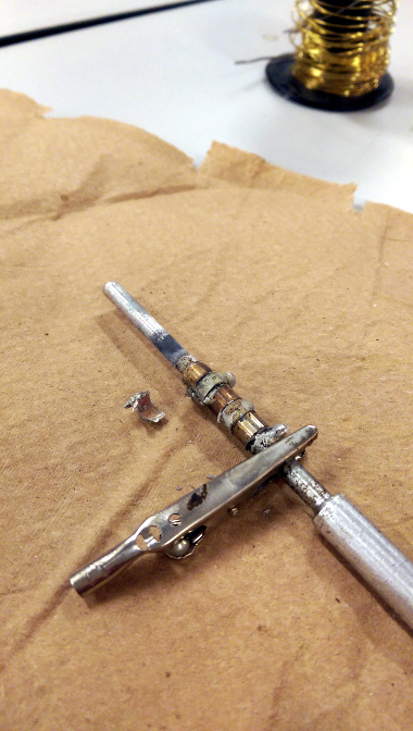
Abandoning superglue, I tried using silver solder. This was a risky prospect, because aluminum forms oxide layers that don’t adhere well to solder, and stainless steel just doesn’t wick until very high heats. So I used a MAPP gas torch, liquid flux, and silver solder, which resulted in…

pen14

My brass rings melted right off the tube. Was not expecting that.


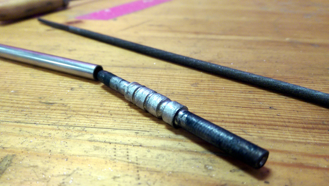
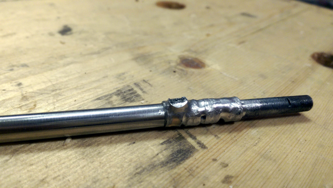
Okay, attempt number five. This was a tube I machined out of mild steel with the brass rings, and only silver solder between them instead of alternating with steel.

pen15

As opposed to stainless steel, mild steel was really easy to work with and soldered to well. It oxidises, though, not acceptable for anything on the outside of the pen. So it needs a sheath on either end.

pen16

And then roughing it out. Superglue works fine for the final steps, because there are no cutting forces trying to tear it apart.

pen17

Filing and finishing it. So much filing. Part of the reason this project took so long is that between each of these steps, there’s one or two hours of filing to make all of my interference fits work.

pen18

Afterwards, I sanded from 180 grit all the way up to 600 and then emery paper. It was mirror finish by the end, and with a little bit of polyurethane varnish used to seal it all in.

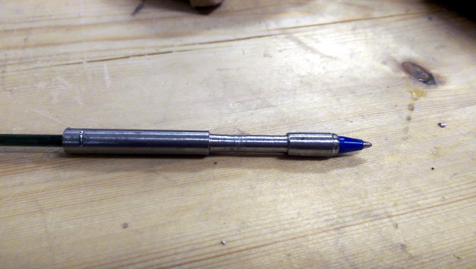
As you can see, the idea is to hold a standard Bic pen cartridge, nothing fancy. Next pen can be more complicated, I wanted this one done quickly. Things I learned:

  • Stainless steel is The Worst
  • Silver solder actually looks great and is easy to work with
  • Stainless steel is so bad
  • Those Youtube videos where they lightly touch the piece with an emery board after they finish machining? They’re cutting like an hour minimum of work out of the video
  • I’m never working with stainless steel again

I’m done with this project, but there are definitely some things I’m not totally happy with, to be fixed for the next one:

  • I built a little pocket clip using spring steel and hammers , but never ended up putting it on
  • There are tool marks on the front portion
  • The very front edges has a little lip from the mandrel deforming it
  • I didn’t let the varnish set properly, so it’s coming off a little
  • There should be some tactile difference where the grip is, it turns out this pen is a little hard to pick up and use without looking at it.

Unpacking WPA2

As discussed in a previous article, WPA2 encryption is comprised of three different algorithms layered on top of each other. I went over them in a very brief overview, so here is a more in-depth discussion on how I optimised and implemented them on an FPGA.

Also linked in that previous article, it’s worth going back and reading this presentation again. It really is a great overview of each of the three algorithms and how they fit together, without muddying the waters with the low-level details.

Disclaimer: This is my process for understanding and breaking them down. I will be using non-standard terminology, and there are certainly other ways of internalising these algorithms. My methods aren’t the only methods.

The lowest building block, SHA1, has four distinct sections stages of note: Load, Process Load, Process Buffer, and Output.

In a completely linear implementation, it would look like this:

SHA1 Linear

I’m assuming a bus width of 32 bits. The input/output blocks on the end are fixed in size, and cannot overlap. Not if we want to maintain half-duplex compatibility with the parent device. That may or may not be important, but it sure does simplify the implementation for now. 165 clock cycles total.

We have a little more wiggle room with the red blocks. Because the buffer can be processed as it is getting populated by the Process Load stage, we can merge them. Extrapolated, and using the input/output as the bottleneck, we come up with this:

SHA1 Parallel (2)


Notice that there’s still only one green section running at any single point along the horizontal. That’s the critical path, and dictates how many parallel operations we want to run at once.

It works out to 106 clock cycles for one cycle, assuming we run 5 hashes in parallel. So, 22 clocks per hash. Way better.

hmacpseudo

The next block up, the HMAC function, contains two SHA1 functions, which is sort of annoying. The second/outer call is also dependent on the output of the first/inner one, so I can’t parallelise that at all. To fill up the 5 SHA1 operations I have going at a time, I must also be running 5 separate HMAC operations.

There is one optimisation to be done, though, mentioned in the presentation. It’s not obvious how it’s useful in a concurrent environment, but bear with me.

Part of the algorithm requires two buffers to contain the ‘secret’ portion of the HMAC input, padded with 0x36 or 0x5c up to 64 bytes. The parent algorithm, PBKDF2, iterates two HMAC functions, 4092 times, all with the same secret variable. That can be calculated once and used for the entire loop.

If everything is done in parallel, then one would expect that the calculation could be done on-the-fly with little to no penalty. When you consider that each round of SHA1 is 64 bytes, however, you realise that a padded 64-byte input message, followed by the ‘secret’ variable requires two complete rounds of the SHA1 function to come up with the final result. But the first round of SHA1 results in the same output, every time, and can be precalculated. This turns the HMAC algo from what is effectively four SHA1 operations into only two.


pbkdf2pseudo


Note that they’ve actually written this algorithm incorrectly, there is an additional XOR to combine each stage of x1/x2 into a final result, but no matter for this discussion.

The PBKDF2 part is by far the most expensive step, because the area of most FPGAs will be too small to unroll 8192 copies of the SHA1 algorithm (which requires minimum (80 words * 4 bytes * 8 bits = 2560) bits of buffer space). One more optimization could be done, given the right conditions, and it’s a doozy:

The final, very last operation in the whole mess is to append x2 to x1. No hashing after that. That means the final output is two groups of 5 words (40 bytes total). This is the Pairwise Master Key. It is statistically unlikely that the first 20 bytes will be correct, but the second group would be wrong. This means that if we have the PMK and only need to verify it, we can do these calculations with exactly half the silicon area, or twice the speed.

Unfortunately, in this particular use-case we don’t have it, but it’s a great trick to keep up our sleeve.


So what do we have in this use-case?


We’ve gone from the wifi SSID and passphrase, known as the master key (MK), and from that, generated the Pre-Shared Key (PSK), which is known as the Pairwise Master Key in this particular implementation of the PBKDF2 algorithm.

To verify the PMK against the passphrase, something called the “Pairwise Key Expansion” is calculated. From the captured WPA2 packets, we have a few variables: client MAC address, AP MAC address, client nonce, AP nonce, and the Message Integrity Check (MIC), packet body.

The first four variables, along with the PMK get combined together in kind of an annoying way, and then compared against the MIC.

They just call it the pseudo-random function (PRF), and it goes kinda like this:

a = "Pairwise key expansion";
b = min(APMac, CMac) . max(APMac, CMac) . \
    min(APNonce, CNonce) . max(APNonce, CNonce);
r = "";
for(i = 0; i < 4; i++) {
    r = r . HMAC_SHA1(PMK, a . "\0" . b . chr(i));
}
return r[0:64];


Yeah, the actual string is used in the PRF.

This gives us the Pairwise Temporal Key (PTK), which is then combined with part of the (encrypted) body of the packet we captured:


mic = HMAC_SHA1(ptk[0:16], data[60:121]);


And then compare this to the MIC we’ve already captured! Easy, right?

No! It’s a huge pain and would add another HMAC_SHA1 block that we don’t really have room for. This will probably be implemented on the microcontroller firmware or the host software of my system.

USB Side-Project

Sometimes I get a little bit inspired by things on the internet. The internet isn’t all bad.


Here are some projects, pictures, or schematics that I like:

http://old.bennahill.com/tsunami/

http://www.piclist.com/techref/io/usb/pcbmaleconn.htm

http://vonkonow.com/wordpress/2012/03/usbserial-pcb/

http://dlnmh9ip6v2uc.cloudfront.net/datasheets/Prototyping/PowerCell-v13.pdf

(That’s mostly a reference for me, for later)


Pretty regularly, I have need of a cheap microcontroller that does one thing only, like output a stepper motor’s step sequence. It would be nice to have a pile of these, and be able to leave them in place, price being insignificant.


A pretty obvious candidate is the PIC18F14K50. It’s an older PIC that costs about $1.50, has a very small package, and speaks USB. I had also planned to draw a USB card edge connector. The advantage of that is that it’s easy (no solder required!), cheap (minus the costs of a slightly longer PCB), and compact. The cons are that it requires an ENIG gold plated finish to prevent contact oxidization, and the FR4 thickness needs to be 2mm, which is not standard, although not super unusual, either.
 

I’ll probably still do that, eventually, but first I got distracted by opening up a USB flashdrive.


Then this happened:


So I sent it off. It’s a hair larger than the original flashdrive PCB because of the programming headers, but it fits.

USB Thing

I used the PIC18F14K50 because I have a pile of them, but if I were to go for an even smaller package, I could fit a flash memory chip on the other side, like the original. That’s a great pathway to a flashdrive that writes a rootkit on-the-fly to data as it gets stored, for example. Scary stuff, and it doesn’t even seem that hard.

A flash memory chip is even pretty bulky, for what it is. By replacing it with a microSD card, there is even more space for other junk. Like using an ESP8266EX for the microcontroller, and drawing a small wifi antenna on the PCB.


There are so many side channels for this project, I don’t even know where to start.

In the meantime, I’ve spun this off into it’s own repo, here.

There’s a quick LED-blink program, but the real fun is in the “HID” projects.


Note the pogo pins I jammed into my PicKit for programming. The slot quite nicely into the programming header, while the board is being powered over USB.


When you plug this in, it appears to be a dud flashdrive. Doesn’t do anything. Until you forget about it and leave it in for ten minutes. At that point, it emulates a HID keyboard, and starts typing commands.

As this is just a test, it types “Windows-R->Notepad->Hello world!”, but it’s a great demonstration of the terrifying stuff you can do with literally 15 hours or less of work.


Keep in mind, I have never worked with USB hardware before. This stuff is not rocket science.


Don’t plug in unknown USB drives, folks!