EDM Prime

One of my theories for rapid PCB prototyping is EDM, or electro-discharge machining. The idea behind EDM is that you have an electrode hooked up to negative voltage, dunk the system in a high impedance fluid, and then put a potential on the metal workpiece. When that electrode is close to the metal and the potential is high enough to ionise a path through the dielectric fluid, an electric arc gets created between them, taking out a chunk of your workpiece.
Basically a spark welder to remove material.
This is often used for removing broken taps from holes or machining very deep, narrows holes with high precision.

I think I can use this to directly erode paths between traces on a sheet of copper-clad.

EDM is one of those strange niche tools that only machinists are really into. The hardcore kind of machinists that don’t really internet well. There seem to be about three resources on the internet for details on the inner workings of these machines: one CNC forum, one thread of a 3D printing forum, and one Yahoo group. None of these are particularly fantastic.
Fortunately, machinists are a lot more into books. Robert Langlois put out a couple how-to manuals in the early 2000s, and Ben Fleming has some much more recently.
Someone got in contact with Langlois recently, and relayed that he lost interest in the project, would definitely like to see Raspberry Pi control of an EDM, and is open sourcing his books. So, naturally, I’ve read those books. I’ve also found some academic papers and expired patents that go over some design constraints.

There really are three major building blocks in building one of these: a CNC platform, the dielectric fluid immersion tank, and the electronics. The mechanical guys have got the first two figured and polished to a degree that I’m not capable of. The circuitry, though, is all extremely simplistic. I think I can add some microcontroller controls and improve hugely on the designs.
Most of the EDM schematics out there are just rectifiers and 555 timer-based pulse circuits.
One of the more sophisticated designs out there, The Garden of EDM by C. Scott Ananian provides an excellent rundown of design decisions, and has some similar ideas to what I’ve come up with independently. His version seems a unnecessarily complicated, though. Especially considering he never actually built his circuit. I’ll start with a much simpler design, offload more to a microcontroller, and end up with more control out of the deal.

Here are some parameters I’m trying to hit:
20-100kHz pulses
20ns rise times or better
Adjustable voltage up to 80VDC
4 amp current max

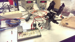
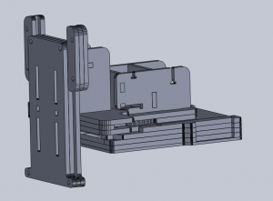
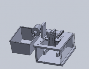
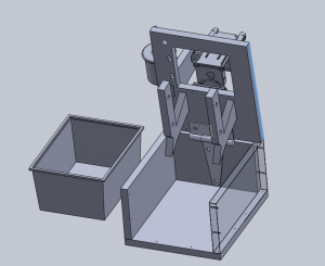
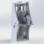
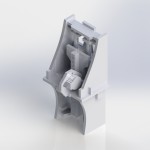
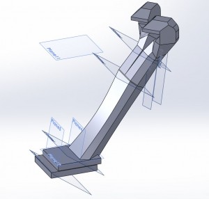
That’s enough substanceless discussion for now. Starting with sink-EDM, the circuitry and mechanical Z-axis go hand-in-hand. I sat down for a few hours and built something in Solidworks:

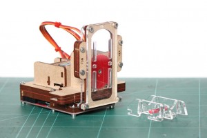
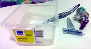
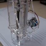
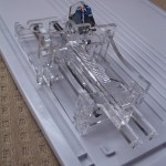
After another few hours, I’ve got it laser cut to get this:

Man, clear acrylic is really hard to photograph properly. Everything was cut on a single try and slotted perfectly into itself on the first try. I’m really quite pleased. The rails are scavenged from an old scanner.

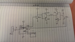
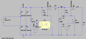
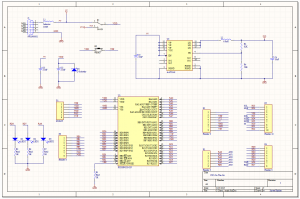
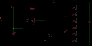
And then alongside that, this is the very first draft of “maybe what I’ll build, unless I have some better ideas”:

EDM Schematic V1

This is a test

Quite a while ago, I did some experimenting with laser etching on glass. The intention was to backlight it and make a large lamp with some LEDs behind a large sheet of laser patterned and frosted glass.
Material costs pushed me towards scaling it way down and designing around a small glass tile that I picked up for a few cents. Just for an initial test, anyway.

The tile I chose is about 96mm², and just a hair under 7.3mm thick at the edges.

For the material acquisition side of things, I hunted for high power LEDs from Dealextreme, one of my favourite sites. They carried some 3W LEDs for a couple bucks, not bad. Then I checked Aliexpress. 1W LEDs were substantially cheaper, but I could only get them in quantities of 100. For $12. So I have some extras.

They measured out at around forward 3.2V. Current is about 120mA when the LEDs appear to be at max brightness. Theoretically they should go up to around 300mA, but this is good enough! I can’t see out of the centre of my vision!

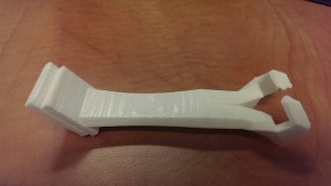
I’m not really a huge fan of 3D printers, but I really wanted to crank this thing out quickly and using one freed up any design limitations for this janky part I needed.

After six quick iterations, I came up with this:

Printed Object

The angles turned out to be tricky to get right, but it worked out. Printed with support material on a Rostock MAX delta printer. The tile is held very securely with no fasteners, perfectly parallel to the base.

Balanced

It even stands up!


Bonus SolidWorks model view:

SW Lamp

For the actual circuit design, I went with all surface mount for easier custom boards, and some free sample chips from TI. See! That program totally works for them, I’m locked into this design now. Actually, it was the best part for the job that I could find. The LM3410, which is a constant current, analog dimming, PWM output boost converter. Yeah, pretty cool.


I found an Eagle library part that had the same footprint as the LM3410, and then I used my standard “print footprints at 1:1” method to find suitable library parts for my Chinese LEDs and salvage-bin inductor with no datasheets.

Parts list:

  • Inductor L1 – CDRH6D28-3R0NC – 3.0uH, 3.0A
    • The datasheet reference designs used anywhere from 4-20uH inductors. Less inductance just means a little more ripple current, which should be okay.
  • Schottkey Diode D1 – B260A-13, rated for 60V reverse voltage, 2A forward current.
  • Zener Diode D2 – I don’t have this yet! Reverse voltage drop between 21-24V. Might have to stack a bunch in series.
  • 1Ω R1, R3 – Two resistors, 1% tolerance, 1206, in parallel to make 0.5Ω
  • 100Ω R2 – 5%, 0805 for voltage overload.

Here are the results of my circuit building:

Lamp Schematic

The schematic is mostly a reference from the datasheet. Max current and voltage limits are a dependent on switching speed, the inductor I used, and the heatsinking of parts, so no hard-and-fast rules. I stretched it to the most high-power LEDs I thought I could get away with. That’s 6. Six LEDs. Worst case scenario, I have to jump one or two of them if everything starts to burn. Best case scenario, I’ve got ten of these boards coming, a dozen inductors, a hundred LEDs, but only three LM3410s.

For this build, I’m trying out the new Dirt Cheap Dirty Board service run by Dangerous Prototypes. I’ve used OSH Park and iTead Studios before, so this will be a fun experiment.


Originally, I was going to etch my own board using a laser cutter and the spraypaint etch resist method. Unfortunately, I have (temporarily, I hope) lost access to the laser cutter. For $14, this seems like a reasonable alternative.


I will update in a month or so, when the PCBs get here.

Knowledge is Power

After pulling apart a NDSL, I know a lot more!


Tracing out the connections, a lot of the LCD pins have a designator silkscreened on, which is totally awesome. I spent a bit of time tracing as many as I could, and then I internetted what I had. That led me to this amazing page, which has the rest of the pin names, but not a lot else relating to this. Totally rad information on other parts of the NDS and GBA systems, though.

Here’s the full(ish) pinout, according to Nintendo:

___NDS-Lite lower screen/lower backlight (P4)________________________________
  1-VDD-5 6-MOD    11-LD1xx 16-LD1xx 21-LD1xx 26-LD1xx 31-LS   36-GND
  2-VDD10 7-GSP    12-LD1xx 17-LD1xx 22-LD1xx 27-LD1xx 32-VSHD 37-COM1
  3-VDD5  8-GCK    13-LD1xx 18-GND   23-LD1xx 28-GND   33-GND  38-LEDA1
  4-GND   9-LD1xx  14-LD1xx 19-LD1xx 24-LD1xx 29-DCLK  34-xx1? 39-LEDC1
  5-VSHD  10-LD1xx 15-LD1xx 20-LD1xx 25-LD1xx 30-SPL   35-REV

That is actually pretty close to the datasheet I’ve been working from. My analysis of where the screens differed was pretty accurate, too, which is cool.

Based on that, here is the NDSL LCD pinout in order, probably, compared to the other one:


Pin Nintendo DS Lite LCD Sharp LQ030B7DD01
1 VDD-5 VDD
2 VDD-10 NC
3 VDD-5 MOD
4 GND SPS
5 VSHD CLS
6 MOD NC
7 SPS VEE
8 CLS VCOM
9 R0 SPL
10 R1 R0
11 R2 R1
12 R3 R2
13 R4 R3
14 R5 R4
15 G0 R5
16 G1 G0
17 G2 G1
18 GND G2
19 G3 G3
20 G4 G4
21 G5 G5
22 B0 B0
23 B1 B1
24 B2 B2
25 B3 B3
26 B4 B4
27 B5 B5
28 GND VSHD
29 DCLK DGND
30 SPL PS
31 LP
32  VSHD DCLK
33 GND VSHA
34 V0
35 V1
36 GND V2
37 V3
38 V4
39 AGND

The signals that don’t directly match the known datasheet are a guess, but usually a pretty good guess (eg. CLS on the datasheet is gate clock, and is in approximately the same pin area as GCK). I’ve gotta go back and check:

  • LS
  • xx1
  • REV
  • LEDA1
  • LEDC1
  • COM1

Figuring out the PCB footprint is also tricky from the component alone, and I made a couple mistakes in my earlier assumptions. Fortunately the PCB gave me a little more information, so this is the Nintendo DS Lite LCD connector. Which both gives me a datasheet, and a 50 cent source for more connectors instead of the Chinese manufacturers that market it specifically for the NDSL and charge $2. EagleCAD has a compatible library model from Omron with the model number “XF2C-3955-41A”.

For the touchscreen connectors, they’re 0.5mm pitch, four contacts. That’s a pretty common sizing, and it’s not even a good idea to use the same connectors. That thing totally disintegrated the first time I looked at it funny. A quick search turns up a decent replacement in both top and bottom contact versions, depending on where I want to mount the connector. Eagle part number “52745-0490” from Molex.

NDSL LCD FFC Design (OR: Working with an unknown TFT screen)

I like acronyms. They make me look smrt.

Designing a board to mate with the Raspberry Pi is pretty straightforward.

It’s mostly just a pass-through board. We need a footprint, though. As far as I know, there are no available PCBs out there that people have used the (nonstandard) Nintendo DS connectors on, so no footprints.

First we try the easy way: Asking the manufacturers directly.
alibaba

That doesn’t work very often. Fun story: I once emailed an industrial control company looking for the models for some of their $5000 3-phase power supplies. Having the files would save me probably half an hour while laying out an equipment rack. Twenty minutes later, the customer support team emailed me the internal engineering model file. Complete with PCB model, populated with all components.

I really really don’t think they were supposed to do that. I thought it was pretty funny.

NDS LCD FFC Connector

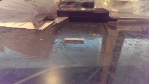
Here’s the LCD connector for the NDS screen. As you can (sort of) see, it’s 20 pins, and measured a little over 11mm from the first to last pins. With a connector that small, though, exact pitches are still hard to be sure about.
And it’s two rows of pins.

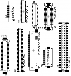
So we go through the Eagle parts libraries looking for something that might work. I kept my eye out for small-pitch 40-pin, double row connector footprints specifically, but I dumped a whole bunch of connectors onto the schematic that might work, after some changes.

Quick layout on the board, and…
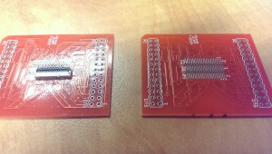
SOIC Test Board

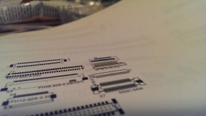
…Print it out 1:1 and see what lines up. I used to think that footprint-measuring PCBs were dumb, but I think I’m coming around. Would save me a few minutes and a little printer ink.

The pins lined up with (one side of) the connector labelled XF3B-5145-31A. It’s a 0.3mm pitch Omron connector.

FFC Printout

Good. Using that information, we draw up the new part, and Bob’s your uncle. I don’t know what that phrase means.

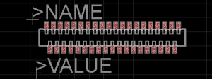
LCD Footprint

Side note: The LCD flex cable is pretty standard, and I may try and find an alternate connector in the future. For this, right now, I just wanted a known-good connector and design a PCB around that instead of ordering a big bag of assorted FFC connectors off Digikey.

After drawing the new library parts (touchscreen connector footprint, too, remember), I need to know how to connect everything. In this case, I have an LCD of uncertain properties, a Raspberry Pi GPIO connector of known properties, and a known resistive touchscreen.

For the touchscreen, it gives an analog value (more on that in a future post), so we’ll need an analog-digital converter to get the values to the GPIO. I’m thinking the SX8652 or AR1011, we’ll see. Digikey has them both inexpensively.

The TFT LCD is a little trickier. I wrote in a previous post that someone found a datasheet for the Sharp LQ030B7DD01 that looked similar, but now that I have the DS screen in my hands, I don’t think it is.

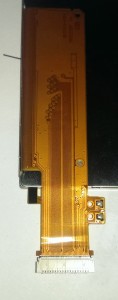
NDSL FFC

From what we can see right here, there are 39 pins. Good.

That huge plane that covers most of the top is probably ground, and is connected to pins 4, 18, 28. and 33. Not good. Assuming pin 1 is on the left, the pins don’t line up properly with any single node.

Even if I have any of the above assumptions wrong, the datasheet lists pins 10 through 27 as RGB data lines. Pin 18 must be independent.

If the right side of that image is pin 1 instead, the above problem still exists. There are only 39 pins on the datasheet, so it seems possible that pin 18, near the centre, could be designated as an extra ground pin, but there are 39 physical pins that correspond to that datasheet, so there isn’t really any wiggle room here.

On the right side of the picture, you can see pins 38 and 39 going to some large pads. Those loop around behind the visible flex cable, and then connect to that one you can see on the right. Looks like a backlight control, probably.

Anyway. Those are the reasons I don’t believe this is the right datasheet, but fortunately, there is a “Sharp” logo on the back of the screen. So I do have a starting point for finding a better match.

Going down the internet rabbithole, I found a German-language forum discussing the LCD, which linked to a now-defunct NDSL hacking site, which was conveniently backed up on the Wayback Machine at archive.org.

During that bout of internetting, I came across an antitrust lawsuit that Sharp was involved with, price fixing these screens alongside Hitachi. That means that both manufacturers were producing LCDs with the same pinouts, so that gives me another lead to a possible datasheet. But anyway, it’s probable that the Sharp LCD is LS030B7DD12F, which has no datasheets available online. The Hitachi counterpart is probably 49N07020132, same story.


I guess I need to actually track down a Nintendo DS Lite and really hack it. Damn.

I like candy. Do you like candy?

At a place that I hang out on very rare occasions, there’s a big red button.

button1

When somebody holds it, it starts up an air raid siren that can get really loud. Unfortunately, it spins up very slowly, so people let off as soon as they figure out what the button does. That results in one tiny little blip of the siren, barely enough to bother anyone. That’s no good at all!

So for this build, I didn’t want to spend very long at it, and attempted to do everything very roughly and as quickly as possible. I found all of the appropriate components kicking around, and designed around those.

Here’s what I came up with:

button2

I found a transformer with outputs that measure at about 12VAC. 10:1 winding ratio, I guess. After rectification and smoothing, it’s a little over 18VDC. On the right side, I used an ALA2F12, a 12V relay. The transistor is a 2N3904, just a very generic NPN BJT because this application doesn’t require anything special.

The original button was just the AC line voltage to the fuse, then through the switch to the load, very very basic.

Okay. Starting from the left:

  • Transformer outputs at 12 volts or so,
  • through the half-wave rectifier diode (1N4007 I think) – results in 12 * root 2, about 18V,
  • big filtering capacitor (200v, 820uF),
  • 1MΩ bleeder resistor so the system doesn’t hold charge indefinitely,
  • original switch (connected to the big red button),
  • 100Ω resistor(to prevent sparks)
  • into timing cap (160v, 220uF) – charges to full very quickly,
  • another bleeder resistor,
  • Rb controlling current going into the transistor’s base (more on this later),
  • BJT  base.
  • At the top: resistor controlling going into the relay coil,
  • relay coil,
  • BJT collector going to ground.

Because I’m abusing a 12V relay by driving it with 18V, I had to compensate for that a little. According to the data sheet, the coil is nominally 272Ω, taking 43mA of current. Ignoring the transistor’s collector-emitter voltage (probably ~0.2V): 18v / 43mA – 272Ω = 146Ω. So I tossed a 150Ω resistor in series with the coil, and it seems to work.

For the base of the transistor, this resistor (along with the capacitor) is what controls the active time of the system. It also controls the maximum current that can conduct through the collector-emitter junction of the 3604 Typically the gain of those are in the 70-100 range, so current going into the base should be Ib = 43mA/100 = 0.43mA. Base-emitter junction is around 0.7v, so the base resistor can be figured out by 18v – 0.7v / Ib when the base cap is fully charged. Overdrive Ib to 1mA to ensure max-on, so I used 18kΩ.

I tested everything to check timing issues, overheating, etc., and it works well. The relay gets latched for about 7 seconds, which is perfect. If I cared about being more precise with that, or wanted to change the timing values, it’s pretty simple to treat that portion as an RC circuit and tweak the resistor or capacitor values.

So I built it

Perfect! Start to finish, took about seven hours. Not including the abortive first attempt last week.

So before, when newcomers pressed the button, there was only a very short blip of the air raid siren. Now, the thing latched for a good seven seconds. And it gets very loud in that time.

I need another dev kit

Recently, I got given an FPGA development kit to continue working on my SHA1 system. The end-goal is to eventually integrate that into a PCI-E card, but we’ll see how that works out.


The FPGA kit I have is the Digilent Basys2, and it uses a Xilinx Spartan 3E chip. The lowest-tier, 100k gate model.


I’ve updated the current code, here, consisting of the parallel behavioral SHA1 implementation, a serial input wrapper that parallelizes the data and acts as an interface, a simulation testbench, and a physical testbench specific to my board. Unfortunately, this code, which is the absolute simplest building block of the final project is about 600% too large for my dev board. It takes up about 12,000 logical slices, and the Spartan 3E version I have only has about 2,000. For further reference, a Papillio Pro, which is very popular right now, uses a version of the Spartan 6 family that has about 9,000 slices.

My goal right now is to, without spending a whole lot of money, to get a development board, or even a bare FPGA on a breakout board with at least 15,000 slices so that I can benchmark this implementation of the algorithm. After I do that with the first iteration, I can write a concurrent version, benchmark it, and start tweaking. I’d really like to get into low-level optimization.

Stretch goals involve getting a massive FPGA to do a lot more with, but those can start to run upwards of $150 just for the chip alone.

I don’t even need to keep these boards, I just need to use them briefly as a proof-of-concept.

Stop-gap PCB creation (has stopped)

Preface:

This is a year-old post that I never published. I guess I was waiting to be able to snap some pictures, but that never happened. Most of these components have been e-wasted by now.

I’ve talked about various avenues of rapid prototyping circuit boards before, and not really come up with any definitive solutions.

My current favourite possibility is using a dye-sublimation printer, but they’re fairly difficult to get ahold of. I’m not willing to throw money at the solution just yet.

In the meantime, one of the more reliable methods is toner transfer, using a clothing iron. There are two easily-controlled variables that affect the transfer quality. There are a lot more than two, but those are the ones that involve a human element.

As a solution to that, I started work on my own laminator. I took the fuser from a laser printer and mounted it to a board.

Mounting and getting it working independently had a fairly involved process. First I needed to drive the motor.

It required a lot of torque and I have no access to any simple motor that can handle that. The only thing I have that comes close is one of my brushless DC motors, but man, I don’t want to use complicated driving circuitry for that. What I ended up doing is mating a simple 12v DC motor to the gearing for one of those motors. I laser cut a bracket that has mounting holes for both sides, ground down a shaft, and it seems to work. A very consistent and slow speed, and huge amounts of torque.

The next step was the heating element. I ran it off one of the 30v supplies we have kicking around, and it got to the “reasonably warm” level while drawing just over 1 amp. Fortunately (or unfortunately, depending on your perspective), a local e-cycle company was closing down and had an impromptu fire-sale. I picked up a 60v power supply that was labelled “broken” for free. Replaced a PTC (that literally crumbled away in my hands), and it was good to go again. The new supply got it to “properly hot” in a minute or less.

The next step was measuring the temperature. The fuser had a thermister output that starting at around 33kohms. As it gets hotter, the resistance drops. I measured around 19kohms when it was “slightly hot”. That’s the totally objective temperature description I’m going with here.

I used a voltage divider with a 100k potentiometer to tune it to 0xFF at room temperature. The reasoning being that I didn’t actually need to know the “proper” lamination temperature, just the relative values that apply to this system.

So I had the whole system, the drive motor, the heater element, the temperature measurement. It turns out that while my system is 0xFF at room temperature, everything melts at 0xA0. That’s not very hot at all! I think. I have no idea what that translates to in real measurements.

There is another printer kicking around that I should be able to pull the fuser out of. The rollers didn’t really feel that hot overall when they melted, so it’s possible that it was just because I wasn’t running the motor at the same time.

Fortunately, there’s no shortage of old laser printers destined for the scrapheap.

Further adventures of implementing SHA1 encryption on an FPGA

A few years ago, I designed and simulated a SHA1 encryption machine using CMOS logic. I actually built everything using Altera’s FPGA tools, Quartus. With standard propagation of the 7400 series, it worked out to about 1.8MHz max clock speed to prevent race conditions.


Implementing the system right in VHDL and running it on the FPGA itself, I think I can get it faster. The previous system also relied on a serial workflow that limited the data to one hash at a time. If I parallelize everything, I can likely get it up to 80 time faster. A very very cursory look suggests that SHA1 has been done a million times by a million different people, but I’m not looking at their work. This isn’t about them.

After trying to figure out how I figured out the SHA1 protocol last time, it looks like the only document I used was the original RFC 3174 spec. There are a lot crappy pseudo-code and diagrams out there, but man, that paper is just so well-written, nothing compares.

I also found an old spreadsheet in my Drive account in which I’d written out the first few rounds of the hashing process.

Initially, because I’m relearning the algorithm at the same time that I’m relearning VHDL, I implemented it completely sequentially. The project is here. It’s a proof-of-concept, not actually something that is usable, at the time of writing. It will likely evolve into something cool.

Vroooom

There isn’t really any story behind this.


I have a joystick module, and it would be pretty simple to hook it up to a motor and use it for a remote control car.


I decided on a few parameters:

  • No microcontroller. Where’s the challenge in that?
  • Joystick wired directly to the car. Wireless can be a stretch goal, this is supposed to be a really quick project.
  • Front/back on the stick will drive 12v DC motors with variable duty cycle PWM for speed control while keeping torque high

This is a reasonably complicated analog circuit, and I really do prefer to simulate my numbers when I do that, just to make sure that I have a valid starting point for real-world tweaking.

I’m not really that keen on diving into SPICE (especially LTspice, which would be my only option, at the moment), but a cursory Internetting around came up with CircuitLab. Now, I’m not normally one to plug some commercial service without very good reason, but this service is seriously pretty great. It’s an online, cloud-based schematic editor and simulator.

I’ve been playing off and on with online services for five or six years, but really nothing has been any good.  But this one is really intuitive, free for non-commercial use, and they don’t even nag me about buying anything, even after detecting that I have an adblocker.


But anyway. I may or may not build this, it was mostly an op-amp and 555-hysteresis exercise.

Here’s the first stage, with a potentiometer(R5) controlling the op-amp output voltage. Varying the voltage adjusts the control voltage that the capacitor is allowed to charge to, causing the output duty cycle to change.

DC Motor - Single stage


Here’s a steady-state simulation of R5 low, PWM output (and therefore DC motor speed) low:

DC Motor Transient Low

R5 high, PWM output high:

DC Motor Transient High


Perfect.


That’s only half the battle, though. I need to get two inverted PWM signals coming off a single potentiometer, centred around the middle.

Part of the challenge of that is that you can’t just duplicated the above circuit. When the pot is involved with both high side(for controlling forward) and low side(for backwards), the circuits are somewhat in parallel.

Some small resistors to ground where needed to mitigate that. Eventually, I got a gorgeous graph that looks like this:

DC Motor Sweep

The important takeaway here is that the output voltage at the joystick-centred position is effectively nil for both sides. Each one respectively ramps up when the potentiometer is shifted to their side.

The 555 output stages aren’t in this simulation because they don’t change from the first circuit.

Here’s the second circuit:

DC Motor Full Schematic


The low-side 555 circuit isn’t shown either because again, doesn’t change.

A couple more notes:

  • I’d actually be driving this circuit with 12v, but capacitor charging rates are all relative, so the timing wouldn’t change.
  • Those two resistors to Vcc and GND, R6 and R9 are to adjust the joystick trim.
  • CircuitLab actually has excellent export options, too. I didn’t use them because I like the gridlines.


Again, this project is mostly just a fun simulation exercise. If I’m ever really hard-up for something to build, I’ve got everything written down here so I can do it. That may never happen, though.

Clearing out the backlog

A couple years ago, I started work on a timelapse camera module. I built one board, came up with some corrections, and designed a better version. Then it stagnated for quite a long time.

A few months ago I checked over the files again and sent them off to a fab shop.

After the new boards arrived, I couldn’t find a local source for some of the components I needed and it sat for a long time again.

A few days ago I found some components that would also (mostly) work, so I started the project up again. Let’s get ‘er done.
 

The goal of the project was to be able to hook into any 2000-era tiny resolution digital camera and take a picture at set intervals. It’s powered by USB, and regulated down to 3.3v that most cameras use. There’s a very simple 7-segment-display-based interface with which to control the timelapse interval.

It’s powered by a PIC microcontroller, and the display is driven by a couple 74HCT164 shift registers by TI. The “HCT” portion of that is key, because these are both wide-voltage range (to be able to run off 3.3v), and fast enough to clock 8 times without visible flicker.


Here’s where I’m at right now:

I don’t have the 3.3v regulator that I designed for, but I found a different one that is adequate, with some bending of pins. None of my capacitors are the right footprint, and I don’t have the right resistor network package. All of these parts are pretty easily available off Newark/Element14, so I’ll have the appropriate parts for my second prototype.


Other than that, it looks pretty good. Keep in mind that I designed this version over a year and a half ago. I’m in a very different place now. Here’s what I would do now (or will do for a redesign):

  • I’ve mostly sworn off resistor network packages.
  • I realize I should have added a couple more decoupling caps.
  • I prefer to use SMD to DIP now.
  • With surface mount, I could also make this whole board much smaller.
  • USB-A male-male cables aren’t really common anymore, it would be much more convenient to use a microUSB port.
  • Driving the camera inputs would probably be safer with a transistor instead of directly from the PIC.
  • I need mounting holes.


I’ve rewritten the software. It stores timer values in EEprom and uses an interrupt to trigger the camera. At a later date, I’ll add in sleep settings for power saving, and control the camera on/off state for the same purpose.


For the interrupt, I want it triggered about every second. It triggers every time the 2-byte Timer1 register overflows. With the maximum prescaling dividing the clock (and register) to one second, I’d have to set the clock speed down to 1MHz. That slows down other parts of the program, enough to make my software-SPI-controlled display have visible flicker. That’s not cool.

To get the proper time, then, I need to count off a bunch of interrupts until I get to 1 second. I’ll calculate a good set of values for Timer1 to do the necessary.

Fosc / 4 = 1MHz

1MHz / 8 prescale = 125kHz

Period = 1 / 125kHz = 8ms

1s / 8ms = 125000 clocks

Say, 125000 / 2 = 62500 clocks

65536 clocks before overflow – 62500 = 3035 starting value (and decrement seconds every other interrupt)

After measuring against a stop watch for two and half minutes, it’s about 3 seconds too fast. That’s 3 / 150 seconds, or about 2%.

So change the starting value to 3035 * 1.02 = 3095.

I’m using the internal oscillator, which tends to be pretty inaccurate. That’s okay, I can tune it. A good way to do that is to take timelapse photos of a clock when I’ve put everything together. I’m curious how much it’ll drift after I calibrate it due to time or temperature. It’ll be an experiment.

Pictures of the build process to follow.


At first, I was lamenting not having proper mounting holes on my PCB. After examining the chassis I had lying around, though, this is perfect. The ribbed interior can hold slices of acrylic, and, properly cut to shape, they’ll sandwich both of the boards, the 7-seg display, and the lens assembly exactly where they need to be. No fasteners, and no unnecessary holes. Perfect.