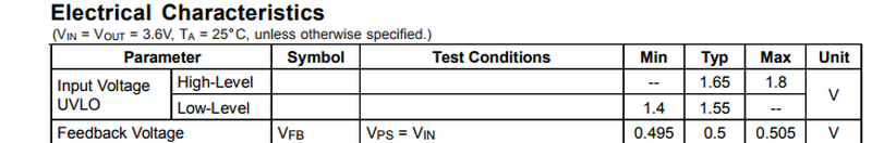
Shallow
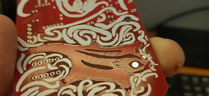
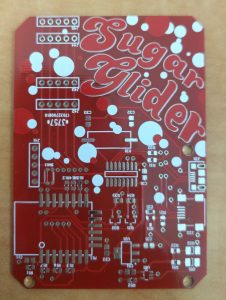
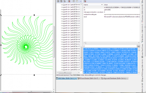
As a test, I designed a nautilus-themed PCB in PCBmodE.
PCBmodE is not your standard ECAD package. It’s a collection of JSON files that get converted into SVG or gerber files.
There are some limited tools to convert SVG files back into JSON, too. It can be thought of as forward- and back-annotation.
There’s no schematic editor. There’s no traditional PCB editor. The only interface is Inkscape itself. (Inkscape is an open-source vector software, like Adobe Illustrator)
The end takeaway is that these circuits are drawn, not engineered.
The whole repo is here. All of the JSON files are the source files, which can then be compiled into SVG (for viewing and some minor edits), or to gerber (for manufacturing).
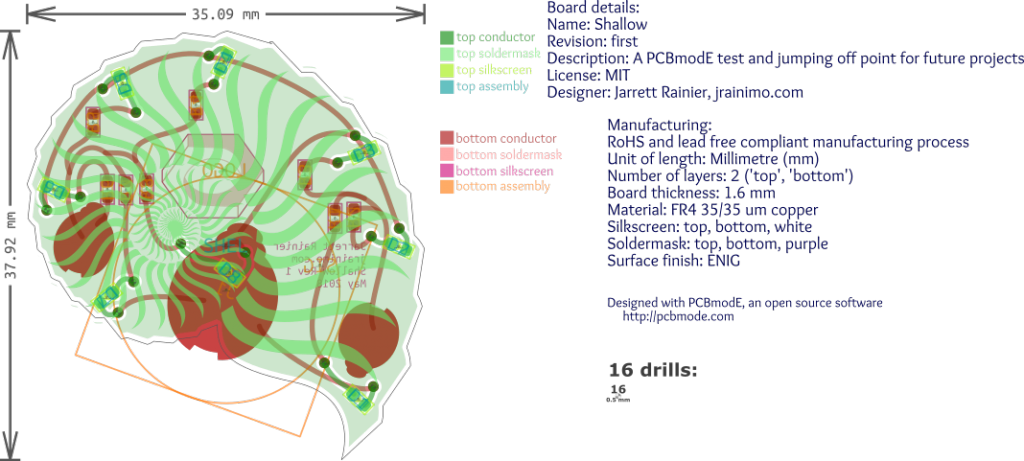
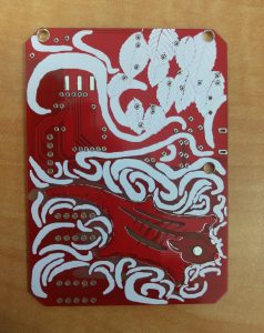
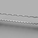
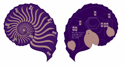
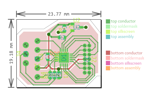
The OSHPark gerber viewer says it’ll look like this:
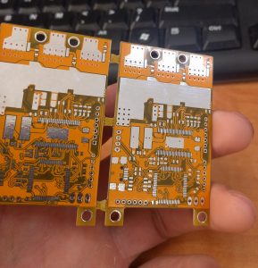
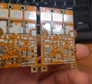
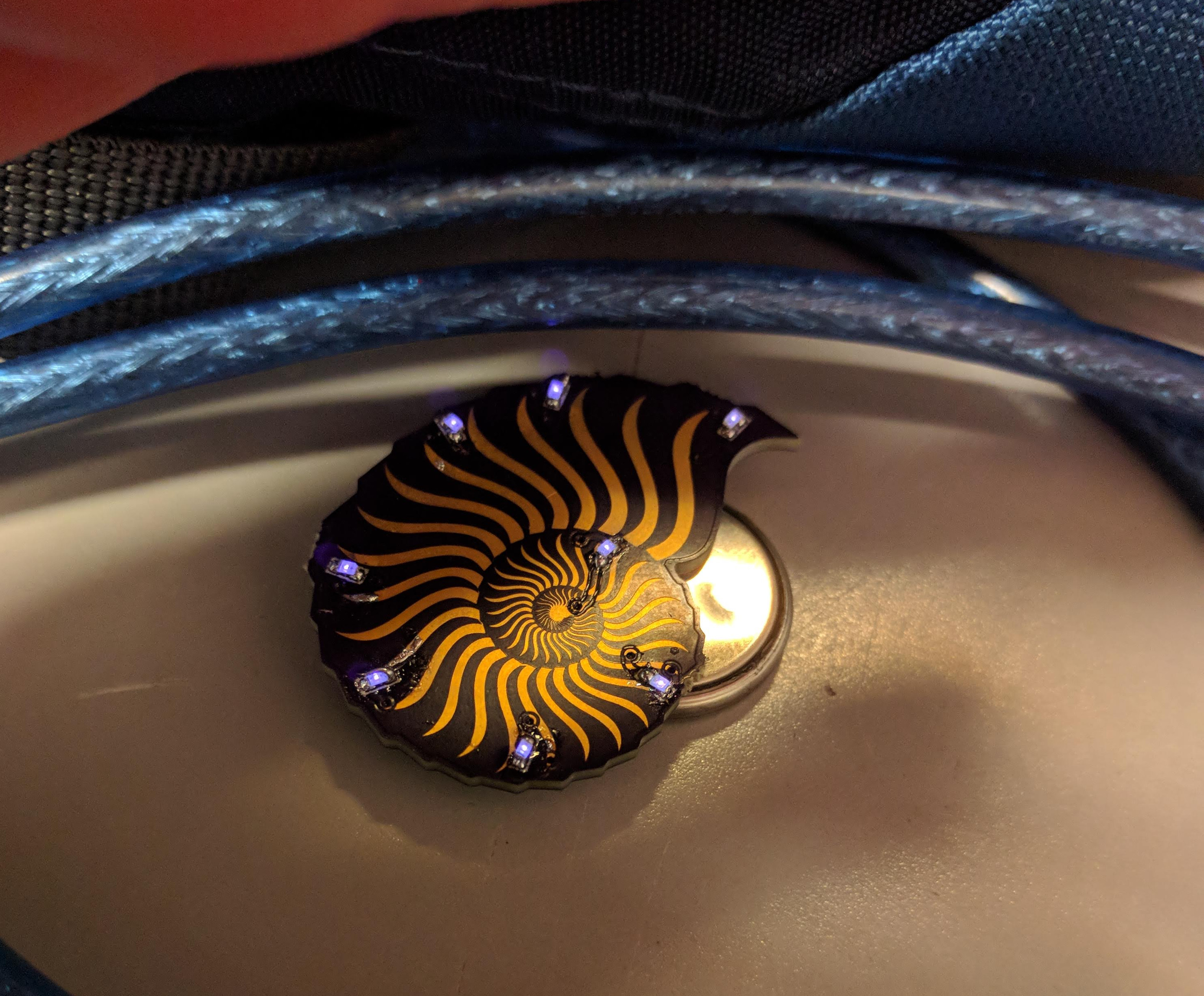
And here is the final board:
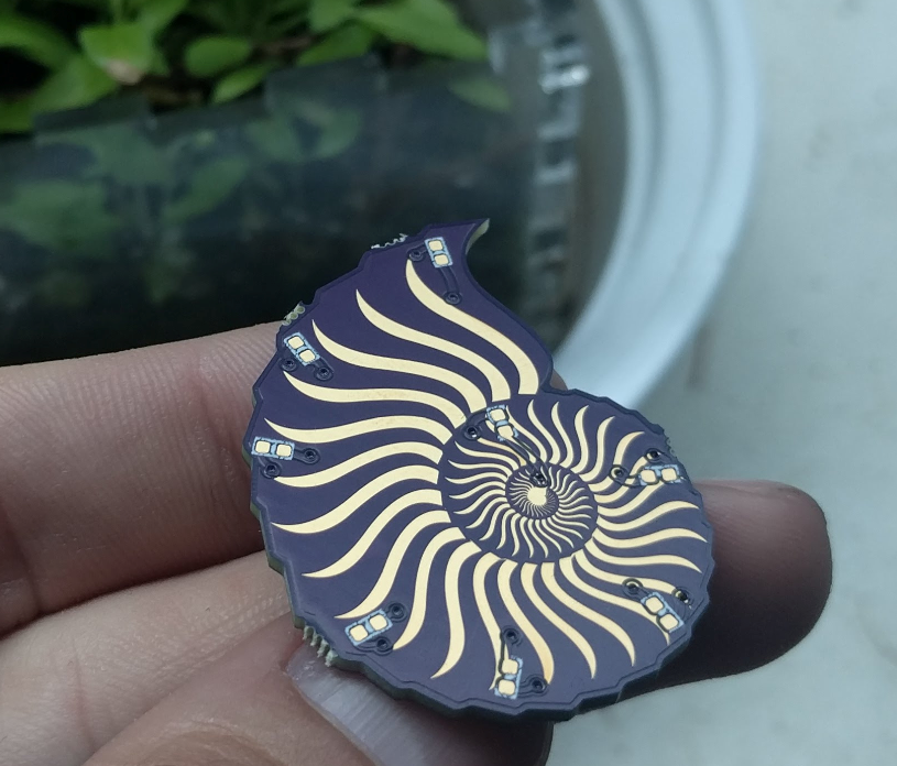
It’s surprisingly difficult to photograph purple LEDs. It was suggested to me that they may have strong UV components that are overexposing that part of the image, so they usually show up as white or very light blue.
Rest assured, they are way more pleasing to the eye in person.
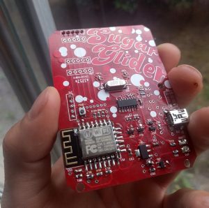
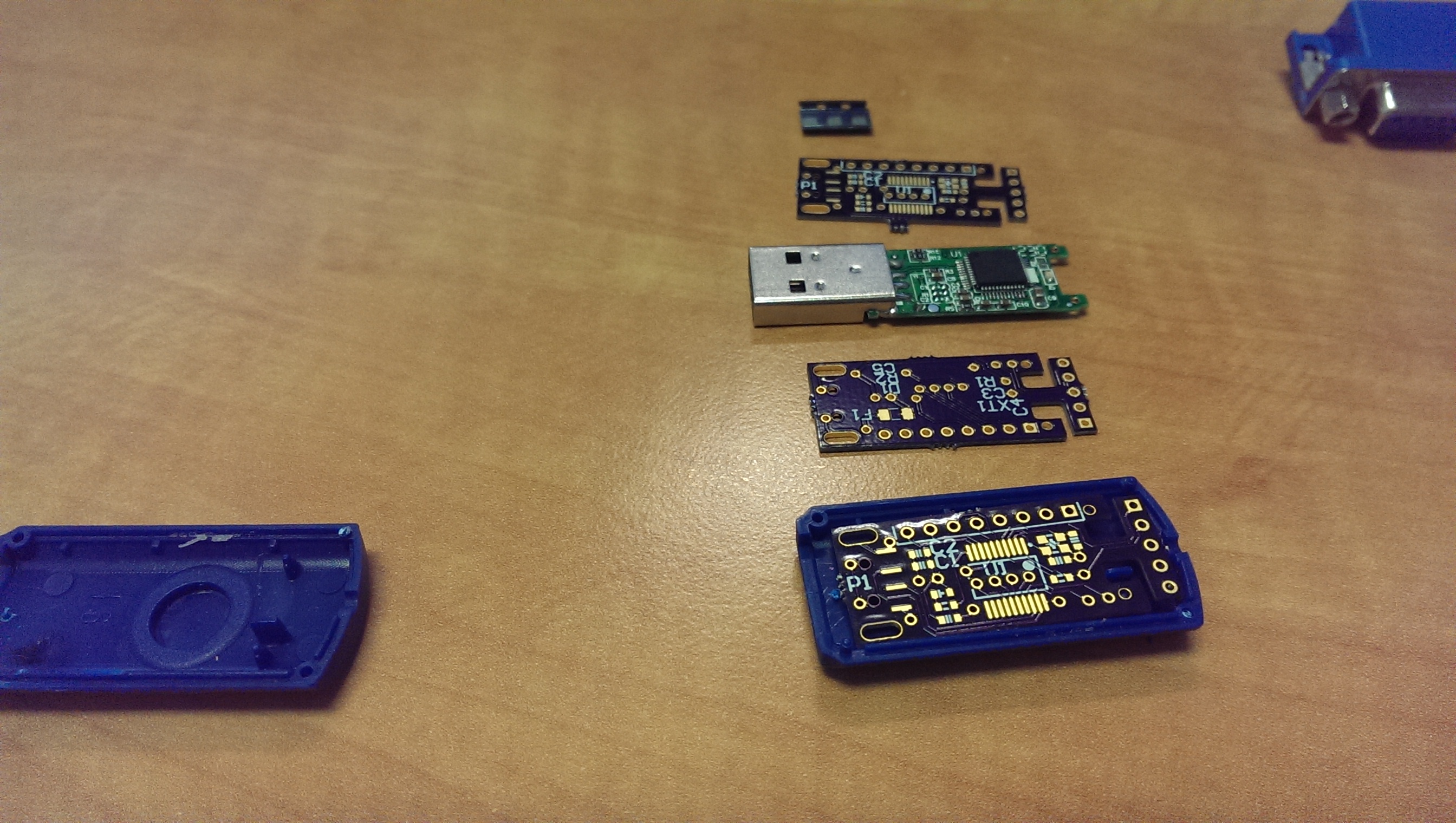
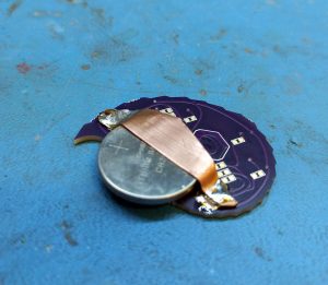
It’s interesting to note that the battery holder footprint was a Boldport component (it looks like a ladybug!). It’s designed for one of those cheap stamped metal CR2032 battery holders, but I don’t have any. It was easier/faster for me to grab some sheet copper and cut out a holder with tin snips.
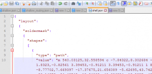
The workflow of PCBmodE is a little bit jarring for someone expecting a standard PCB tool. It’s all laid out in the official docs, but I didn’t believe it until I tried it. Editing JSON files is almost the only way to interact with the software. You edit, compile, and view it in Inkscape. Some very small amount of things – Component position and traces, mainly – can be extracted back into JSON, but that’s it.
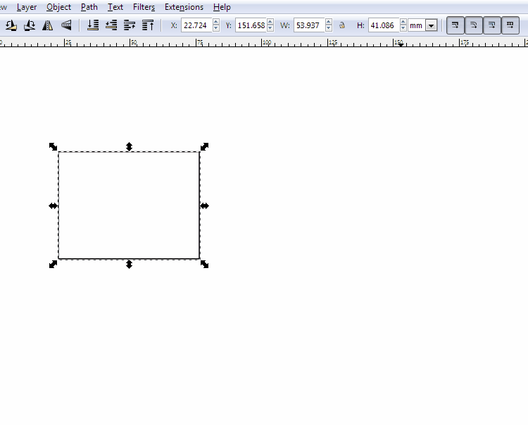
Even for outlines, the best method is to draw them in Inkscape, then copy the SVG paths and then paste them into the appropriate JSON:
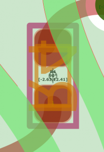
For moving components around, there are a lot of SVG layers present for each component, but the extract command only seems to care about the origin. That little dot in the middle:
Three last things:
There’s also no “generate new board” command. Official recommended procedure is to fork one of the existing boards and modify. The docs are outdated, the sample is for an old version of PCBmodE that won’t work. I like BINCO for something really simple, or The Lady for something that uses every trick in the book.
Don’t use the official repo. This fork(as of June 2018) is the almost-official dev branch that has a lot of improvements (including Python 3!), and presumably will be merged back into mainline at some point. This command will install the proper one:
pip install git+https://github.com/threebytesfull/pcbmode.git@improve-test-coverage
And, finally, there is one issue that will prevent manufacturable gerbers. I described it here.
The next step
So, obviously this software requires some fussing, initially. It’s pretty nice once you have it set up, though. No issues, as long as you know what they are ahead of time.
What’s still a pain for daily use, however, is building usable circuits. Lacking a schematic and having to hand-draw traces as vector paths is painful.
So I quickly grabbed the first complete PCB available in Upverter, my LightBeam board. And then I wrote a conversion tool.
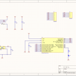
Here it is in Upverter: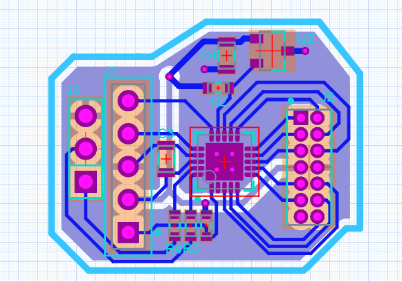
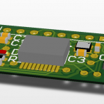
And then in PCBmodE:
Workflow is now: Make a PCB in Upverter (or import it from something else!), Export as OpenJSON, convert it with my tool, then edit the PCBmodE JSON files as required to prettify them up, and transform them into something amazing.
The tool is here, pull requests / issues welcome. Only a small amount of available things to convert are completed, there’s lots more work that could be done.