Dumping Firmware With a 555

Voltage glitching, also called fault injection, is the process of dumping the energy on a microcontroller’s power rail very briefly – Just enough to cause a glitch, where it skips an instruction, rather than causing a brown-out-induced reset.

I first learned about the technique in connection with the Chip Whisperer, which is an FPGA-based board with all the bells and whistles. It’s quite expensive, and like any other situation where you add an FPGA, very complicated. Naturally, that has elevated it to a level above what mere mortals can perform in the limited free time we have.

After knowing about this, and having it in the back of my mind for several years, I finally have a good use-case that can justify spending some time on this. I have a pile of generic STM8-based devices, and while I have written some of my own alternative firmware, I’d love to be able to dump the original flash to revert them back to factory code.

The function of the device doesn’t matter, that’s not the point of this exercise.

Some quick searching for options leads to this recent write-up, which is sparse on details, but serves as excellent inspiration that this task is very doable.

A few architecture notes:

The STM8 has a Read Out Protection bit in the configuration area of its flash memory. When the programmer attempts to read out the flash memory, the bootloader first checks this bit, and if it’s cleared, it starts reading out the flash to the programmer. If it’s set, it just reads out zeroes. Write capability is never blocked – That is, you can still write a zero to that ROP, and then the microcontroller will be “unlocked”, but it does clear the program memory, too.

One of the pins on STM8s is called VCAP, and it’s attached to the internal voltage regulator. The CPU runs on this voltage rail, not the actual voltage that is provided to the IC’s power pins. The pin is intended to be connected to a decoupling capacitor, and that provides an perfect spot to inject my glitches. Most microcontrollers also have something called Brown-Out Resets: When the input voltage rails sags too low, the peripheral triggers, and resets the microcontroller. Obviously, this is something we want to avoid, and using the VCAP pin should help with that.

In terms of glitching, there are two important considerations:

The glitch must start at the same time or during the cycle in which the CPU is trying to read the ROP bit, and the glitch must not last long enough to trigger the BOR or to make any other important instructions fail. It’s not easy to know these exact timings, so any reasonable values must be tried, essentially brute forcing the process.

Now, the logical way to do this would be to use an external microcontroller to wait for the programmer to reset the system, wait a set period of time, and then trigger the output transistor to glitch the voltage rail. That’s boring! You know what else can do that? That’s right, a pair of 555s.

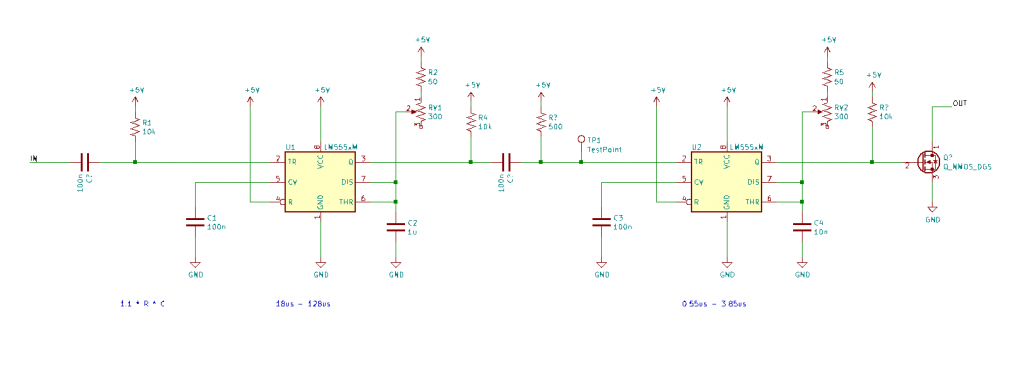
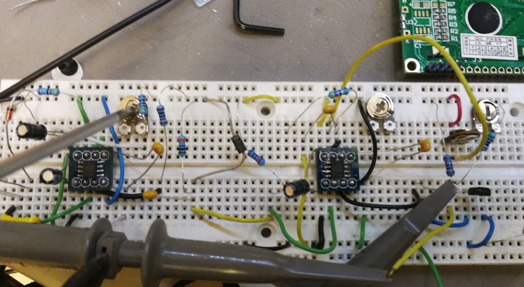
Here are two 555s set up as monostable pulse generators. The input is the RST line on the STM8 programmer. The first 555 then sets the delay. The second 555 sets the length of the output pulse. Both of these timings are controller by a different potentiometer. These then go to a MOSFET that dumps the energy stored in the internal voltage regulator cap.

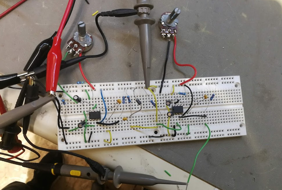
After building it with larger-than-designed time values and testing it to prove that the waveform looks as expected, we solve the next hurdle:

To figure out decent ranges for the potentiometers, my STM8 board runs at 8MHz, which means that each clock cycle takes 125ns. The STM8 requires at least 2 clock cycles for each instructions (one for retrieval and one for execution), and more for instructions with multiple bytes or arguments. So, ballparking, we need a pulse that’s anywhere from 0.2us to 1.2us or so.

One problem with a typical 555 is that it can only generate pulses as small as 10us. Fortunately, I have a pair of high speed versions up my sleeve, the LMC555. It has a 10ns minimum pulse instead, which is very zippy. They’re SMD only, so they get popped onto a breakout board to fit the breadboard, and replaced. Some other components got tweaked too, as I played around more.


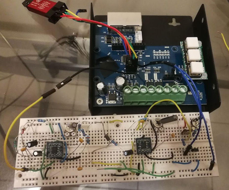
Now on to the programmer. I’m using a standard STLink V2, which speaks the SWIM protocol that allows programming and reading of the STM8’s flash.

With a little bit of bit of Python and stm8flash, we get this:


import subprocess
# .\stm8flash.exe -c stlinkv2 -p stm8s105?4 -r out.bin -b 1
out = b'\x00'
while out == b'\x00':
subprocess.run(['stm8flash.exe', '-c', 'stlinkv2', '-p', 'stm8s105?4', '-r', 'out.bin', '-b', '1'])
f=open("out.bin","rb")
out = f.read(1)
print(out)
subprocess.run(['stm8flash.exe', '-c', 'stlinkv2', '-p', 'stm8s105?4', '-r', 'out.bin'])


In PC applications, writing text to console is a surprisingly slow process, so a low-effort tweak I made to make the loop run faster is to remove the flash utility’s console logging, just by removing some lines here.

So, all set up, potentiometer on the left controls the delay, pot on the right controls pulse length.

And, bam.

Firmware dumping with a 555.


Well, not that fast. It took about 45 minutes of fiddling with the knobs until all its secrets were unlocked. I’d sweep the right knob the whole way, then tweak the left knob very slightly, then sweep the right knob again. It only really worked because the knobs only had to be within the right range for a very brief period of time. It only had to work once.

Would this have been easier with a microcontroller? Oh yes, of course. But that’s not nearly as interesting.

Chromaticity

Here is a brief overview of how light and colour work, in the context of LED lighting.

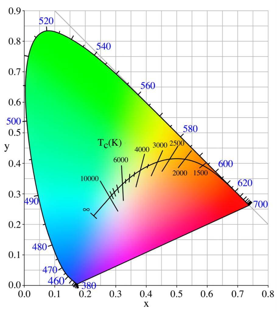
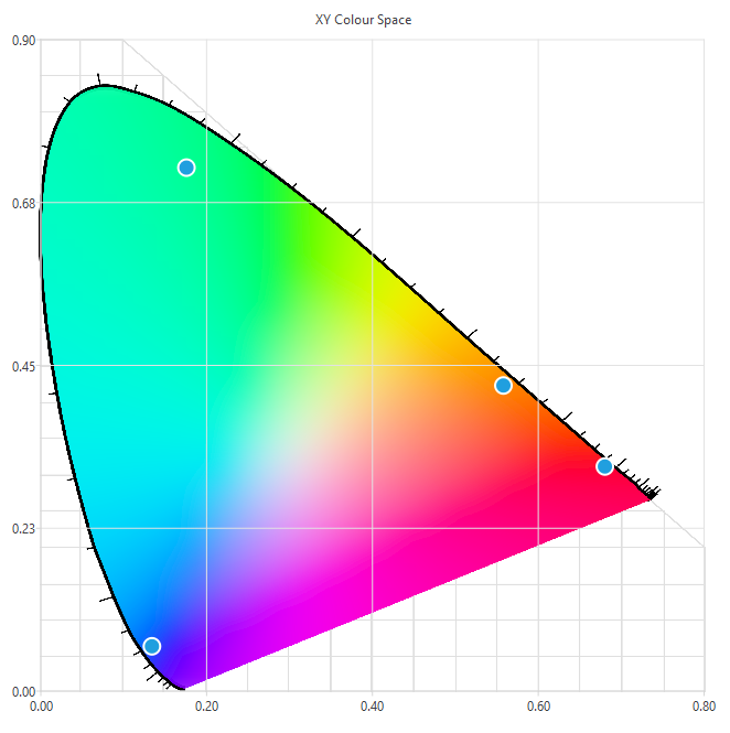
We’ll mostly be discussing the CIE 1931 colour space, with reference to the chromaticity diagram, shown below.

This is the 1931 version. Newer versions that look slightly different have come out, but the general intent is the same, and they are all used for different calculations. The 1931 version is “good enough” and is universally the one that is referred to when a colour is described in xy coordinates.

The points along the edge are pure visible wavelengths (displayed in nanometres). Anything inside the diagram is some mixture of the wavelengths.

Computer monitors don’t have the same kind of visible range as your eyes, so the colour space diagram above is just a representation, not the actual colours that you would be able to see if it were displayed side-by-side with the actual light wavelength.

There’s a curve along the centre, called the black body curve, that represents “white” light. White can be many different things – Typical incandescent bulbs are around 2500K, towards the right (warm) side of the black body curve. Daylight is very cold, with lots of blue components, towards the left. As long as it’s along that curve, it can be considered “white”. The vertical-ish lines indicate where that particular temperature extends, if a given data point isn’t exactly on the line. Duv, or “delta u,v” is a measurement describing the point’s distance from the line.

In terms of white LEDs, there will typically be a “warm white”, also called “tungsten”, and a “cool white”, called “daylight”. As shown by the black body curve, if you have both LEDs, you can’t interpolate between the two of them and expect the light output to follow the curve. It will be a direct line between the two. There are a couple solutions to this, and an easy cheat is to explore the strategy that one of the industry leaders is utilising.
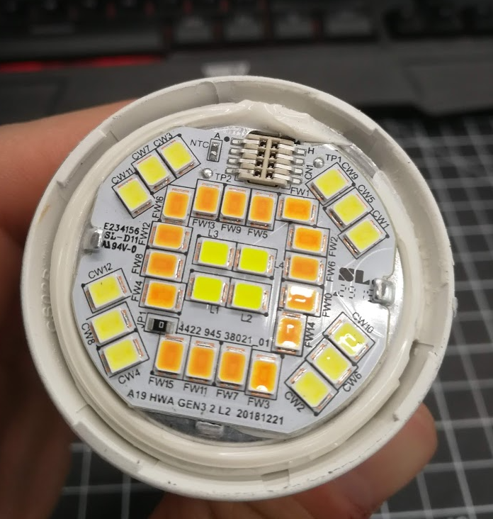
The Philips Hue tunable white smartbulbs are excellent. I’ve taken apart a handful of smartbulbs, and the Hue has the largest quantity of LEDs I’ve seen(read: brightest), as well as using a few tricks to get better light quality than any other system I’ve seen.

The daylight LEDs, labeled “CW”, and tungsten LEDs, in this case labeled “FW”, (we’ll get back to that) are fairly standard. In the centre is where it gets interesting, with the LEDs labeled “L”. This is lime green.

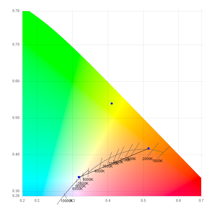
Here is a closeup of those LEDs plotted on an XY graph, with the black body curve, and an interpolation line between them:

With both of the tungsten and daylight LEDs located on the black body curve, fading in between the two will drag the light significantly away from what we perceive as “white”, essentially making the light look magenta. The lime LEDs, towards the top of the graph, are perfectly situated to pull the light output back onto the curve when the bulb is at an intermediate temperature. Some further investigation into the meaning of the LED designators on the PCB, “FW”, reveals that some LED manufacturers with that particular temperature of LED call it “flame white”. It’s substantially warmer than most bicolour white LED tapes, at around 2200K. Mint LEDs are also sometimes used for the same purpose as lime LEDs. Mint has similar spectral components to lime, but with a little more blue components, moving their xy coordinates a little more towards the bottom-left.
Here they are next to a high quality warm/cool (bicolour) LED tape:

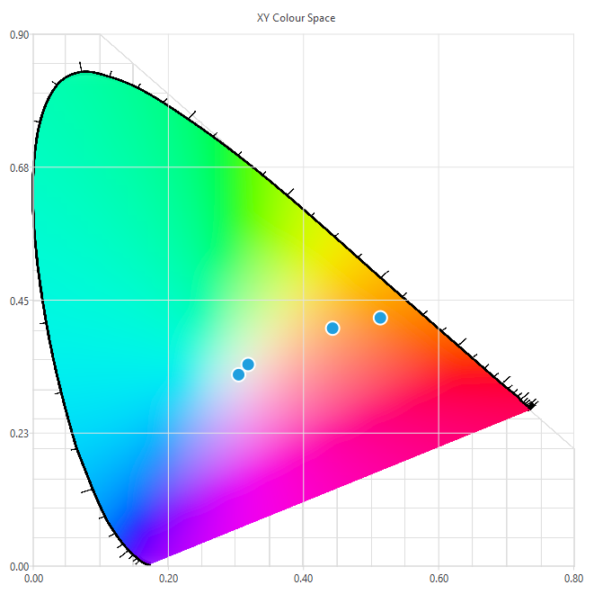
From left to right: my daylight, Philips daylight, my tungsten, and Philips flame. Daylights are fairly similar, within binning and measurement tolerances. My tungsten LED is 2600K, showing how far the Philips flame LED is into the red spectrum. Another strategy for getting temperature that warm is to add an amber LED.

Tungsten, flame, and amber, left to right respectively:

Tungsten LED can be combined with amber to get a warmer (lower) temperature. Amber has an additional purpose: Standard RGB gamuts don’t have a whole lot of range in between the red and the green colours, which can be filled out with the added amber channel. More on this in a bit.

“Gamut” is the displayable area made possible by mixing the available colours. Displayable points drawn with each primary colour, and the available gamut is any point within the area.

Here’s a typical RGB LED tape.

And their spectral distributions:

This green has a slightly wider spectrum than the other primaries, so it doesn’t fit as nicely on the edge of the xy graph. It’s made up of mostly 520 nm and 540 nm components.

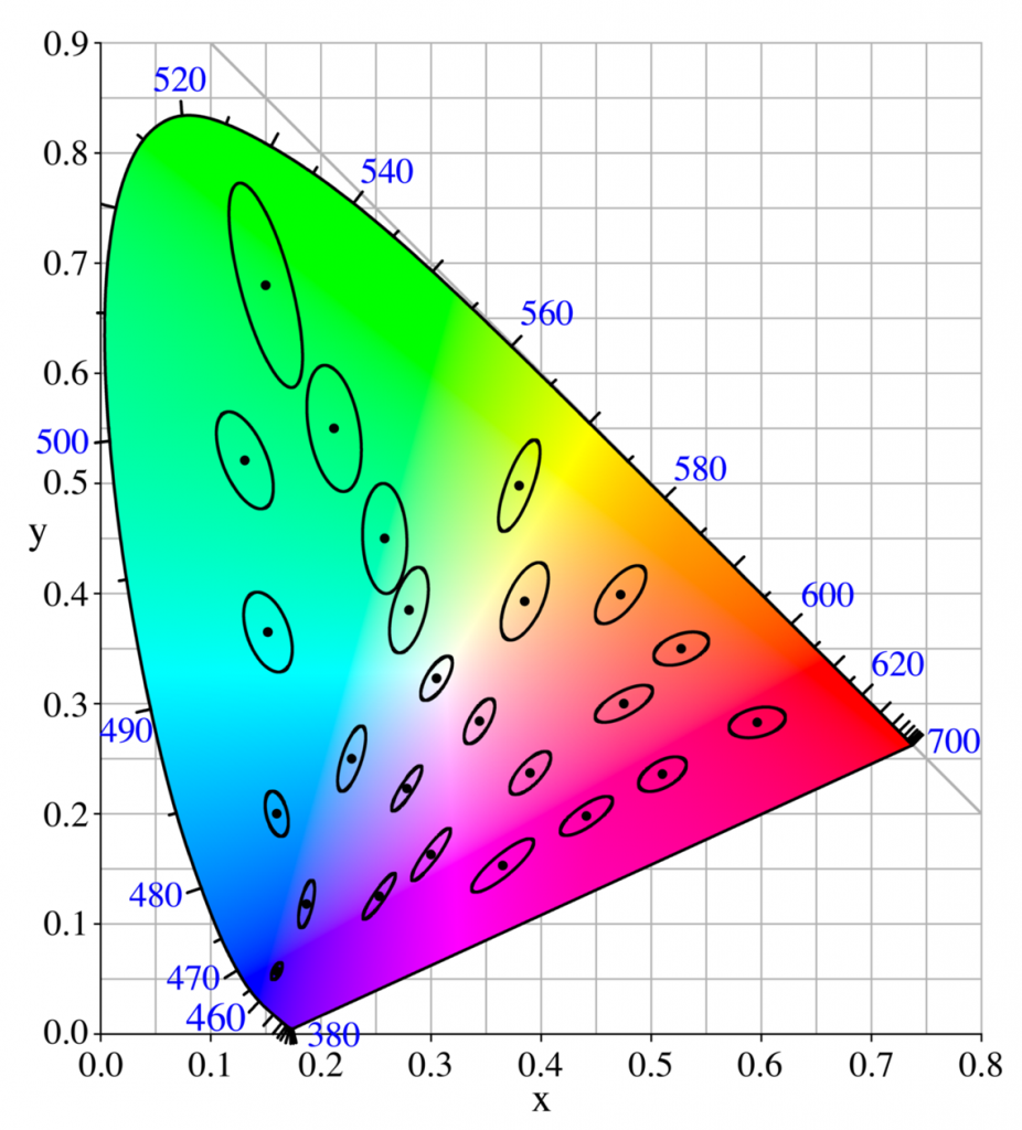
The MacAdam ellipse is a graphical representation of what observers see as “one colour”. That is, anything in the ellipses shown appear to be the same colour to a regular person. This particular image is only the results from one participant in the study, so it shouldn’t be taken as definitive, but it does show trends that can provide actionable insights. The shapes are also exaggerated by about ten times for ease of clarity.

The ellipses tend to flow in the direction of the blue-red line, for example, showing only a few different perceptible shades in between those two primary colours. Red to green however, particularly in the red to yellow region, are extremely granular. This is where amber comes in.


The amber gives additional granularity in the existing gamut region where our eyes are very sensitive, and in the space where the gap between the RGB peaks is largest.

Emerald green, at 560nm, is another LED that would help fill out the spectrum gaps, providing more range towards the green part of the red-green line. Emerald and amber doesn’t alter the overall gamut significantly, however. There are areas without coverage on all sides of our gamut triangle, but the area to the left of the blue-green line is the most significant. This could be supplemented by InGaN cyan LEDs, at 505nm. That will be the topic of future experiments.

For reference, here is a graph of all of the colours measured and discussed.


Watching Plants Grow


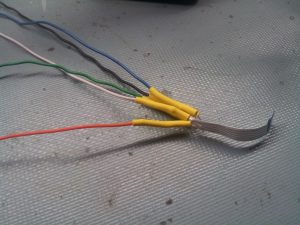
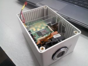
I’ve been into timelapse photograpy for a long time, often focused on driving the cost down by hacking existing digital cameras.

That follow up post (already written almost two years after the original work) promised project pictures that were never delivered, so here, I went spelunking in some nearly decade-old backups for them.


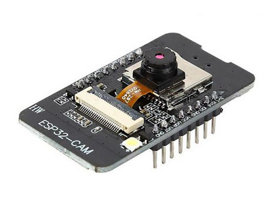
Recently, I came across the ESP32-Cam, which basically hits all of the cost/hardware requirements I was aiming for, nearly a decade ago.

It uses an Espressif ESP32, which I’m very familiar/comfortable with, and is about $6. The camera sensor is 2MP, which is small for images, but fine for video.

There are a lot of timelapse projects out there using this board, but none of them really have the features I’m looking for. Espressif even has an official “webcam” codebase that others have packaged up into cool projects. But here are my requirements:

  • A web interface to control capture / timing parameters
  • Serving up images over the web interface to check that those parameters are good
  • Saving images to SD card
  • Nonvolatile storage of the parameters, along with the current snapshot number, in order to gracefully recover from power failure
  • SD card images available to download over the web interface
  • Over-the-air updating
  • Reasonably well-laid out codebase that’s easy to hack on

Essentially, I want to be able to plug this into a hard-to-reach closet and not have to ever physically touch it again. Lots of projects have a subset of these features, but nothing has hit it all, that I have seen.

One of the other ideas I had to improve upon the typical timelapse design was to get the ESP32 periodically grabbing the real-world time from NTP servers. It’s set to run every half an hour, which is probably too often to make a difference that overcome the latency from hitting the NTP server. Regardless, it should keep average timelapse interval perfect over a long period of time.

So I hacked something together. Originally I used PlatformIO with the Arduino framework, because it’s quicker to get a project off the ground than the official Espressif ESP-IDF. The branch is still there, but I abandoned it after running into issues with partitioning, OTA updating, and the additional PSRAM hardware all working together. The main branch uses the ESP-IDF now.

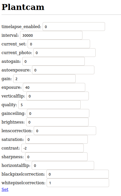
It’s essentially a webserver that controls the camera. You can open up a page and modify settings, including timelapse intervals:


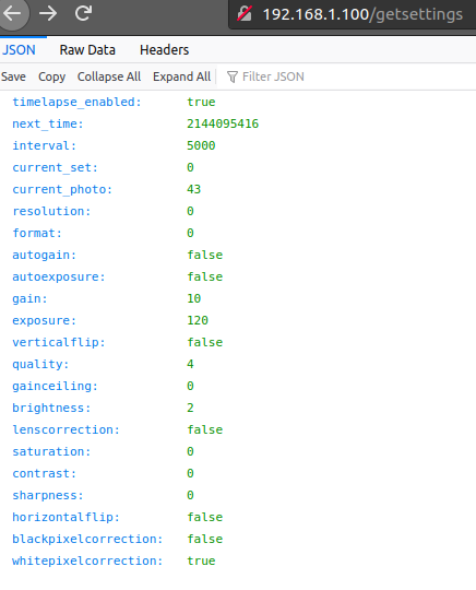
You can also get existing parameters:


And snap takes a one-off photo to check your setup without touching anything. That made this super easy to tweak with one hand, while holding a laptop with the other.

When a sequence is done, it’s easiest to grab the SD card and plug it into a computer to copy over the files. For longer sequences, maybe to check progress, it is totally possible to grab the images over the web interface. Just slow.

To stitch together all the images, initially I used this command:

ffmpeg -r 30 -start_number 1 -i %06d.jpg -vcodec mpeg4 -vf "transpose=1" -y movie.mp4

That results in a pixelated and honestly pretty crummy output. It’s fast, though.

This got much better results:

ffmpeg -start_number 1 -r:v "480/1" -i %06d.jpg -pix_fmt yuv420p -c:v libx264 -preset slow -vf "transpose=1" -y -f mp4 movie.mp4

ffmpeg is a little inscrutable, so the parameters that require tweaking warrant an explanation. Order matters, too – Some of the parameters affect the input, some affect the output, depending on position.

-r:v is the input frame rate, relative to the base (25 FPS) framerate. So a 250 frame video with -r:v 25/1 would be 10 seconds, while setting it to -r:v 50/1 would result in a 5 second video.

The -vf transpose option rotates the video. The ESP32-Cam’s camera is mounted sideways, but that’s a minor irritation.

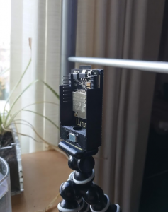
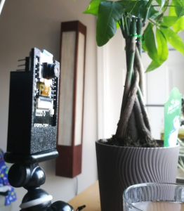
To mount the device, tripods are the obvious choice. I created a quick, minimalist enclosure that allows access to the GPIO pins, SD card, reset button, and fits a 1/4″-20 nut that is compatible with most tripods. A Gorillapod, in my case.


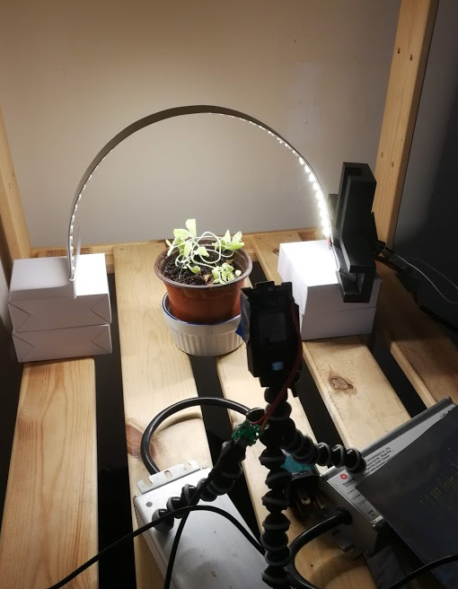
For the video posted at the top of the page, here is the setup:


It was done with a picture taken every 40 seconds, 8 second exposure, low gain and brightness.

ffmpeg -start_number 1 -r:v "120/1" -i %06d.jpg -c:v libx264 -preset slow -vf "transpose=1" -y -t 00:00:08 -f mp4 movie.mp4


The -t option sets the end-time, there was a lot of “content plant” at the end that wasn’t moving much.

Future goals might include shoving the whole mess into a closet, along with timed control of the lights and a watering pump, and leaving it for a month.

POV Globe – Electronics


This is a fairly old project that I just wanted to document to current-state and provide a conclusion. See here for the old logs.
Some of the original design goals for this project were ease of design, and manufacturabilty. Ideally, the design would be clean and turnkey enough for me to be able to at least sell the populated PCB as part of a kit. I also didn’t want to spend a lot of time doing anything cutting edge enough to turn into a time consuming side project, as some of my designs are wont to do.

So here is where I started.

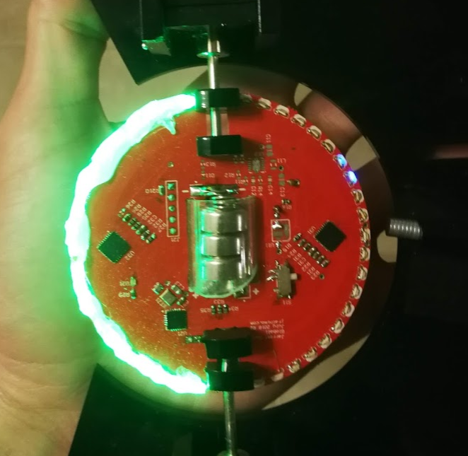
The board is 7cm in diameter with 0805 side-mount LEDs all around the perimeter, green on one side, blue on the other. The LEDs were too easy to see individually (right), so I used hot glue to create a diffusion layer (left).

In the centre, I decided to go the easy route and make the board battery powered. The cutout can hold three LR44 batteries in series.

After some hemming and hawing about how to mount them exactly, I found an acrylic tube with a 12mm ID (just barely larger than the batteries), cut a slope into one side so that it can be inserted into the slot and then rotated to lock in. On the PCB, there is battery spring on one side, and some copper braid on the other to hold the batteries tight and make electrical contact. This solution works better than it has any right to, it is fantastic but blows my “manufacturable” requirement right out of the water.
For driving my LEDs – twenty per semicircle – I used a TLC5947. It’s a constant current, 24 channel PWM LED driver, controlled over SPI(a requirement for speed). There are two of them, and they seemed to work well, with one caveat that I’ll get into in a bit.

There is an interesting power section that I never ended up populating. The goal with it was to have a switch mode power supply attempting to boost the battery voltage to 4 or 4.5v from whatever voltage the batteries sag to. The idea being that with fresh batteries, it wouldn’t be doing much of anything, but as the battery runs down (internal resistance gets higher), the power stage attempts to pull more and more current to keep the output rail steady. The circuit ended up working fine with all of that jumpered over and direct from the battery, but it was an option in case that hadn’t turned out.

I also had a clever system on there to ensure proper polarity to my circuit regardless of how the batteries were hooked up, but again, didn’t matter enough for this version to use.

The TLC5947 has an SPI output pin to allow chaining multiple chips together, but naturally, it would halve the refresh rate I’d be able to get. I ran a trace between the two chips, just in case, but I was also able to avoid using that. The dual effective SPI ports I managed to get working(written about in a previous log) saved me from that.

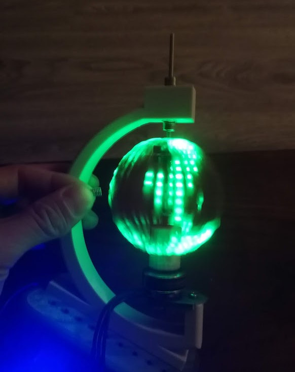
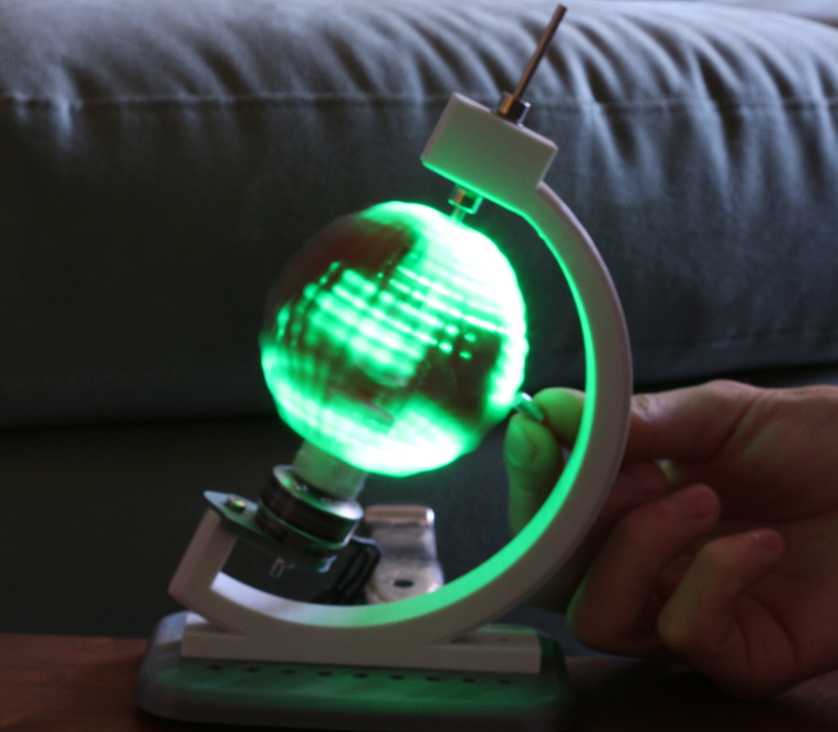
Early tests were promising – I quickly got a recognisable image of the world showing.

Introducing blue turned it into an unrecognizable mess, though. All further testing stuck to green, for now. The problem is that my hot glue light diffusion is too good, and allows light to be directed back through the sphere. Some sort of baffle on the inner side of the LEDs is needed.

An additional problem that I hinted at in the last logs is that my vertical resolution isn’t really high enough. The world map is recognisable, if you know what you’re looking for, but it isn’t fantastic.

And the final problem, the real deal killer: the TLC5947 blanks its output before displaying the next value. That is, a channel displaying 255 (full on) when a new value is sent to it, even if the new value is the same. It will go 255->0->255. That’s why you can see vertical gaps in all the images I’ve posted. This is mentioned nowhere in the documentation, and is just poor design. So future version will have to rethink this portion, too.


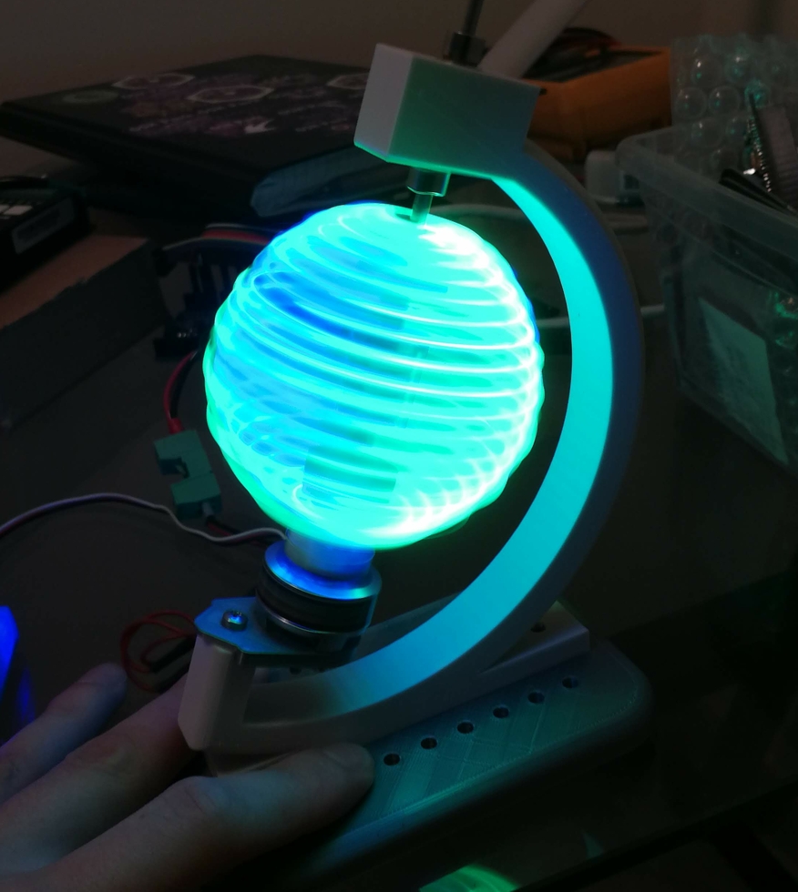
For the mechanicals, due to an unfortunate move, the old system got a little bit damaged and I 3D printed a replacement. This one also uses a direct drive brushless DC motor instead of the old brushed motor and DC motor. Again, just for fewer components and faster to put together.


It worked well, other than some harmonics causing a lot of vibrations on some narrow bands of frequency. Future versions would also have a proper magnet holder, my hand is not a permanent solution.

A Matter of Time

I’m on another clock kick. More of a wristwatch this time.

The dream is to have a couple metal bars floating in oil, and when a button is pressed, they float to the appropriate hour and minute positions.
For an initial version, I’m paring this way down to just a single indicator hand.

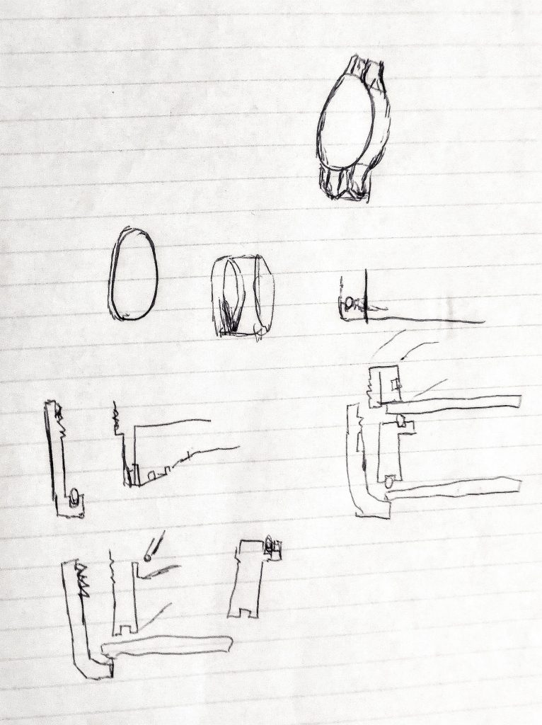
On the mechanical side, I start with some preliminary sketches.

There were many more, with very little polish in any of them. They’re just to get the mechanicals down and direct the overall thrust of the design.

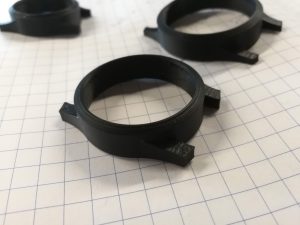
Watch crystals are quite inexpensive from China, so I picked up a selection of sizes, and while waiting for shipping, I modeled and 3D printed some tests for the three most likely candidates. Shown here are cases I designed for sizes 30mm, 34mm, and 38mm faceplates, but you really can’t tell that they’re different sizes in pictures. The 38mm one seemed to fit best on my wrist, so that’s what I went with.

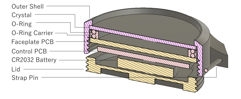
Rolling my sketches into the CAD, I came up with this:

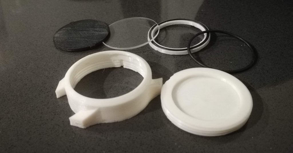
The main body is just a shell with internal threads, and inside there’s a stack-up consisting of:

  • 1.2mm crystal face
  • 37mm OD x 1.5mm o-ring
  • Double sided o-ring retainer
  • Another o-ring
  • 15x3x1mm neodymium magnet
  • Faceplate PCB
  • Control PCB
  • Coin cell battery
  • Threaded cap

Dimensionally, it’s a very tight system. It doesn’t really fit with the battery, so stuff will have to be moved around. The o-rings are there to seal in the oil, which is kinda fun.

Jumping to the electrical side, I need some electromagnets.

A guy named Carl Bugeja has designed coils drawn out in PCB traces to make a PCB motor. He shows off the design a lot here.

Included, naturally, are a set of gerbers which were worth ordering to play around with.

I tossed a magnet on there and was able make it jump around the coils using a small bench power supply. The resistance at each phase was about 12 ohm, the same value that Carl Bugeja measured. Each phase does go through three entire coils, however, so assume 4 ohms per coil.

The coil pattern is illustrated quite well with Carl’s coloured gerber export:

Application of the right hand rule shows that as current goes in a clockwise spiral direction (curl your right-hand fingers in that direction), your thumb will point in the direction of the magnetic field, out of the screen. Interestingly, the ordering of the coils on the layers isn’t from top to bottom. Carl ordered it from layer 1(top)->layer 3->layer 2->layer 4(bottom). Probably to (very very slightly) increase the length of the current path and therefore the resistance of the coil.

To drive a coil with any polarity we like, we need a standard H-bridge circuit. A future version might do some interesting stuff with that, so the fine control that an H-bridge provides is kinda cool. Generally an H-bridge consists of a couple matched pairs of transistors of opposite substrate. Poking around, there’s a single chip MOSFET solution that looks suitable, the VT6M1.

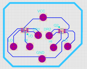
So here’s a quick PCB layout of how that would work:

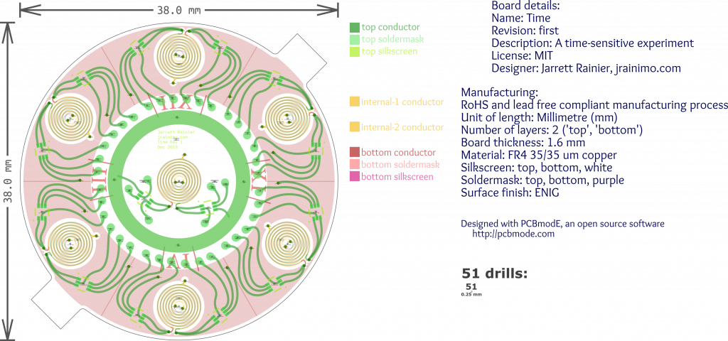
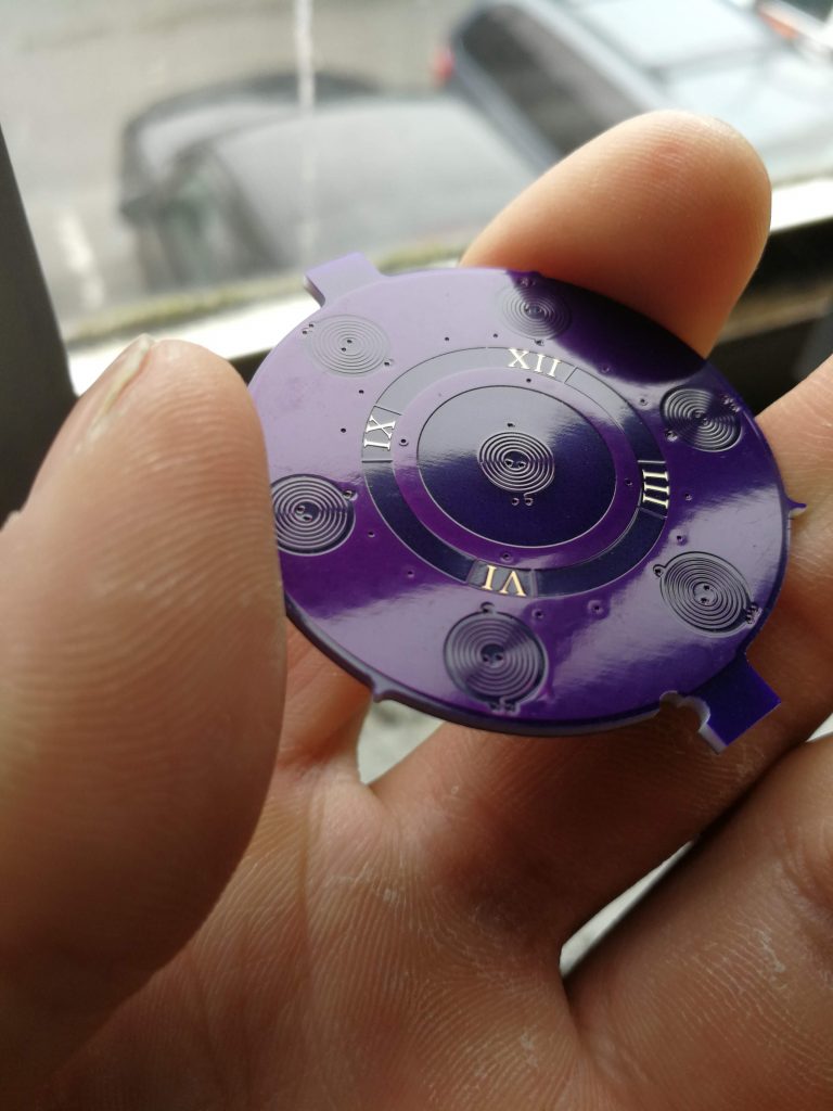
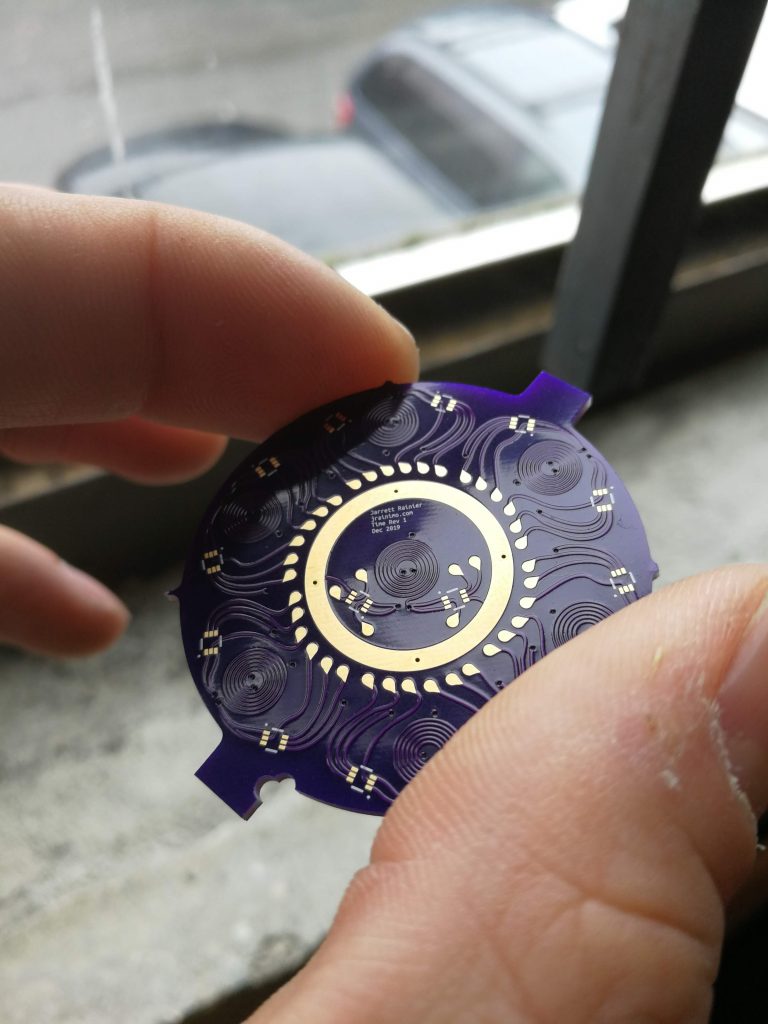
But of course, just dropping that into a board is boring! We’re going to make a pretty PCB, we might as well go all the way! I’ve spoken before about PCBModE. Using my tool to convert the above PCB into a compatible format, I pull it into PCBModE, cleaned it up, added some electromagnetic spirals, and a little bit of flair. There are solder pads to hook this PCB up to another PCB, containing all the brains.

Figuring out a compact way to drive all those connections is somewhat challenging. With six coils around the perimeter and one in the centre, a “drive high” and “drive low” connection for each side, there are 28 signals, plus power and ground. All of those need to be transferred out to a “controller” PCB, so I added those green teardrop solder pads. The idea being that pins are to be soldered onto them, and then pushed into through-holes on the controller PCB.

For the controller, after all of the through-holes that connect to the above-mentioned solder pads are placed, space is very tight! Investigation of various shift registers and their sizing yields no encouraging results. NXP has a cool line of miniature 74HC series logic, but even those don’t fit in my given space.

Fortunately, there is a nice STM32 part I was able to squeeze in.

Despite actually being designed in ECAD software, I think it turned out quite beautiful in its own way.

Some first revision woes:

In retrospect, this was a terrible way to design the electronics. By putting the MOSFETs on the faceplate PCB, I maximised connections needing to cross to the other PCB, and minimised space on the controller by filling it up with through-holes. By crossing with the coil connections directly, I would have needed only two wires per coil, instead of the six that the H-bridge is requiring (plus grounds).

An unregulated coin cell is just about the worst possible power supply for a miniature, portable, long-running device that can’t be opened easily, and leaks oil when it does get opened.

Additionally, I was rushed to get PCBs out and forgot to add a button to activate the watch face.

Next version, with more time, will include improvements for all of the above, as well as a proper external RTC, and LiPo battery circuitry.

Jumping back into the mechanical side:

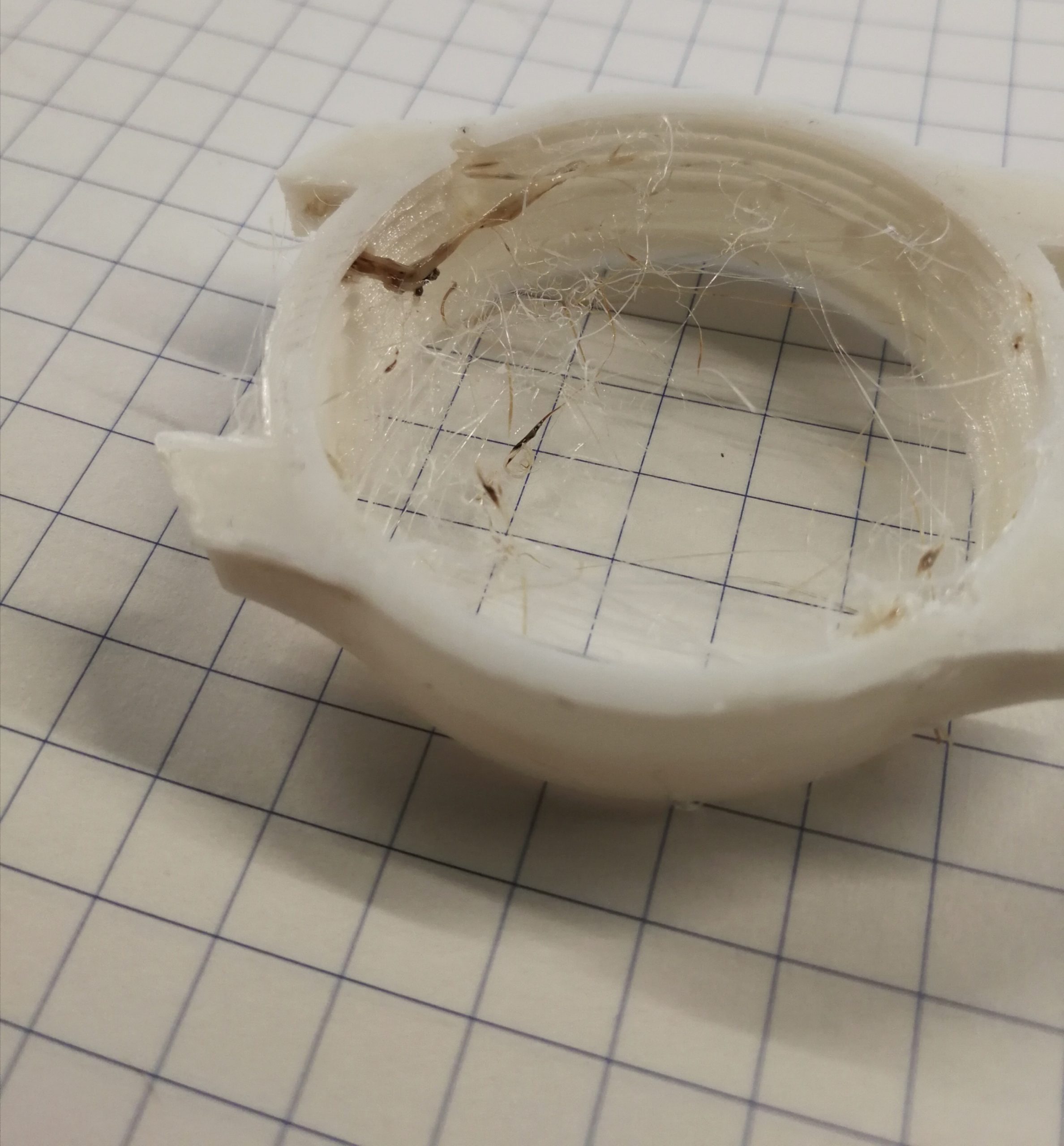
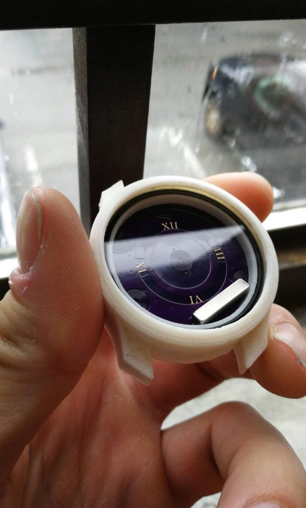
Everything was 3D printed to test fit. Surprisingly enough, threads worked pretty well. There was a ton of stringing in the internal threads, though.

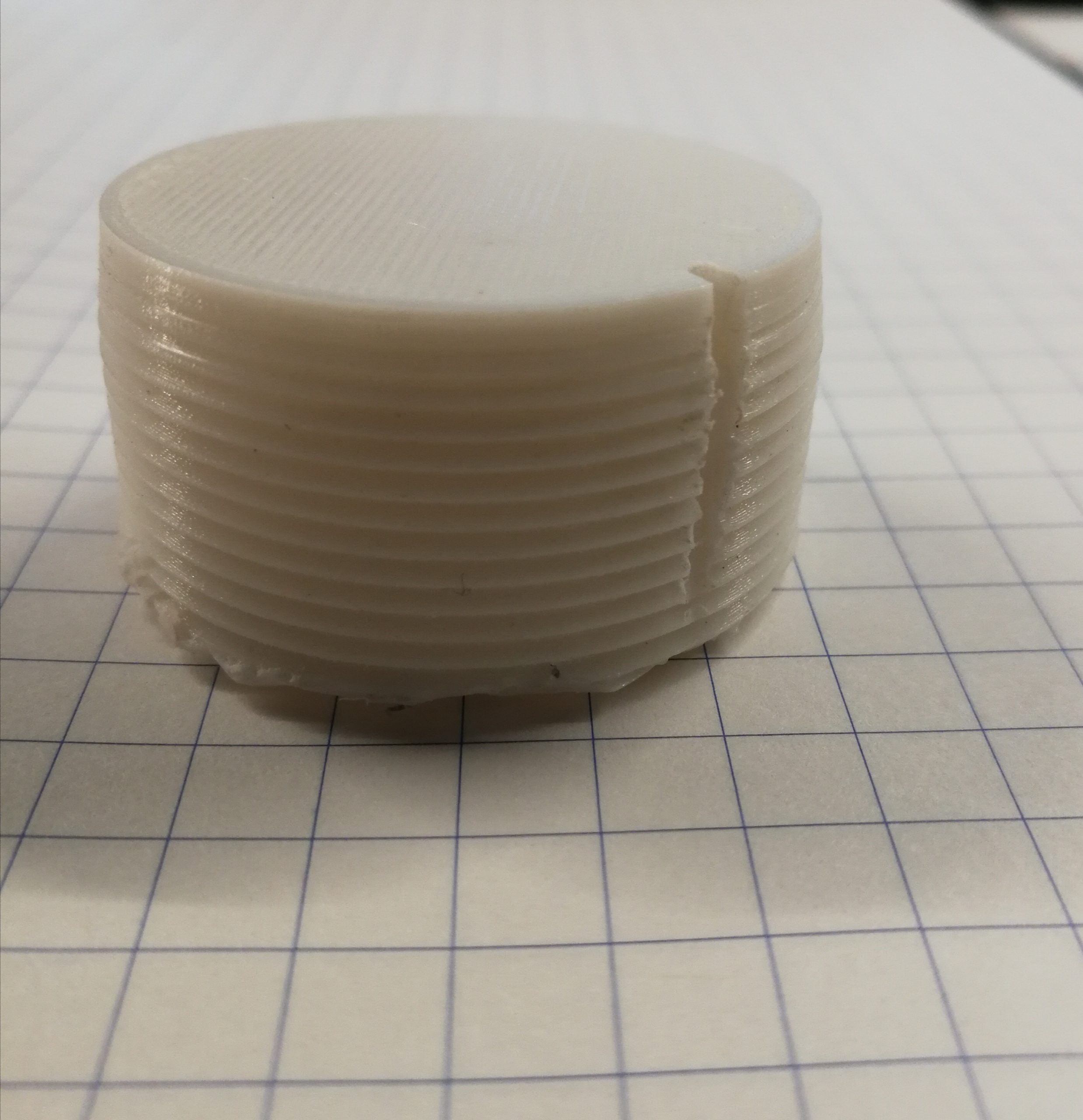
Initially, I was using a knife to clean those up, but that got old quick. Additionally, oozing from the print of the outer threads made it a little tough to mate for the first few cycles. So I printed a tap. You can see the taper on the leading threads, and the notch to clear out the chips.

That worked great! Passing it through the system a couple times made the threads work easily.

Here all the non-electrical components:


Here is the faceplate PCB:


And, assembled:

Testing the coils directly with a benchtop power supply once again made the magnets jump around.

And then adding the H bridge transistors and testing with a low current signal to control the direction of the magnetic field.

Status: super cool. Listen to that click!

For prototyping, everything is 3D printed. The goal would to mill it all out of aluminum and then anodise it dark blue.

The o-ring holder needs to be lathed or otherwise made out of a solid material, too. 3D printed parts are going to have a bad time if I try to use them to seal an oil filled cavity with porous plastic.


I got the endorphin hit I needed out of this for now, though – Some interesting concepts have been demonstrated, and perhaps I’ll come back to it another day to add polish.

Infin1D

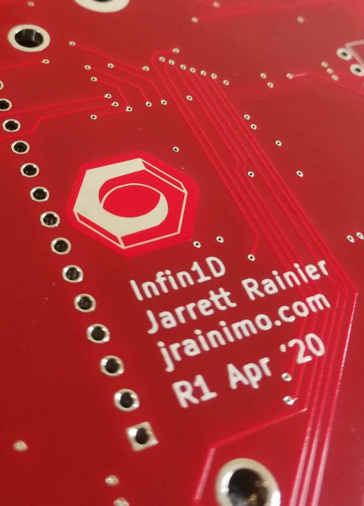
This is a follow up from Infin1D, Rev 0.5, where I threw together a proof of concept in a few hours. This is the one where I spent some actual time on it and built a base that, while still quite rough, can be incrementally improved to arrive at a final product.

This miiight have been the original inspiration I saw, but the video link is unfortunately dead.

Right off the bat, I should mention that PCBWay kindly sponsored the 4 layer PCB for this. In addition to using them for most of my personal stuff, I get more complicated professional boards assembled by them as well. The quality, speed, price, and communication are all better than what I’ve gotten domestically. So I’m genuinely happy to plug them, they rock.


On to it:

I mentioned previously that I’d like to use a scanner sensor instead of the easy line sensor module I had before. That previous module was 128 pixels long, greyscale, and $20, but also well documented, ubiquitous, and easy to use (mechanically and programmatically).

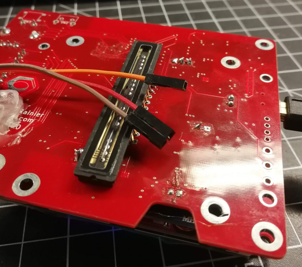
A linear CCD sensor out of a scanner, on the other hand, is almost the complete opposite. It’s huge (107,000 pixels long), poorly documented, electrically hard to control, full RGB, requires external optics, and needs to be mounted to a circuit board. It is also only really available via Taobao, but it is about $7 in singles. Or at least, the one I chose is.

I started by scavenging a bunch of scanners and seeing what was inside. Most of them happened to be the Epson Perfection 1250. I guess it was just an insanely popular scanner.

Searching “Epson Perfection 1250 Service Manual” yields excellent results, so this particular RGB linear CCD is a 22-pin package called ILX555K.

The main processor chip on the PCB is the National (now TI) LM9833, which is a little ridiculous. It contains an analog CCD reader, DRAM storage, high current stepper motor outputs, a USB interface, and even extra helper functions like paper load detect. Basically a single-chip scanner brain.

Initially, I didn’t even have to do any proper hardware hacking (sad day), because there are Linux drivers to talk directly to the chip. It uses something called SANE, an easy Linux scanner interface. SANE is actually a really nice codebase to hack on. Well laid out, clear, and simple.

There are also convenient Python bindings!

First:
sudo apt-get install python-dev libsane-dev sane-utils
git clone https://github.com/python-pillow/Sane
cd Sane python setup.py build
sudo python setup.py install
sudo pip install pillow
sudo pip install numpy
sudo mount --bind /dev/bus /proc/bus
sudo ln -s /sys/kernel/debug/usb/devices /proc/bus/usb/devices
sudo sane-find-scanner
> ...
> (vendor=0x04b8 [EPSON], product=0x010f [EPSON Scanner 010F]) at libusb:001:002
> ...
sudo nano /etc/sane.d/plustek.conf

That file gets modified with the found USB vendor/product/etc info.

And you’re done!

Running scanimage will run the scanner, including homing and making the carriage move, but it doesn’t provide the granularity we need. The source for that provides detail around line 1862, probably calling feed() or reset() / initialise cmd. Sending the initialise byte for a long scanner homing sequence is still pretty high level, so it must be handled within the IC.

That was a fun detour, but ultimately not what I wanted out of the system.

So I threw together a really quick PCB, and I made many mistakes. But that’s okay, that’s what revision 1 is for.

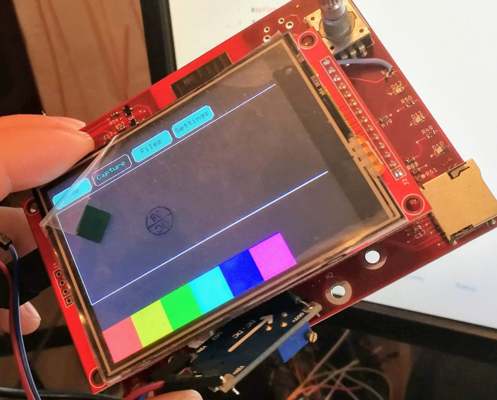
And it works! My initial firmware can display images and I also wrote a bitmap generator to save to the SD card.

A rudimentary interface:

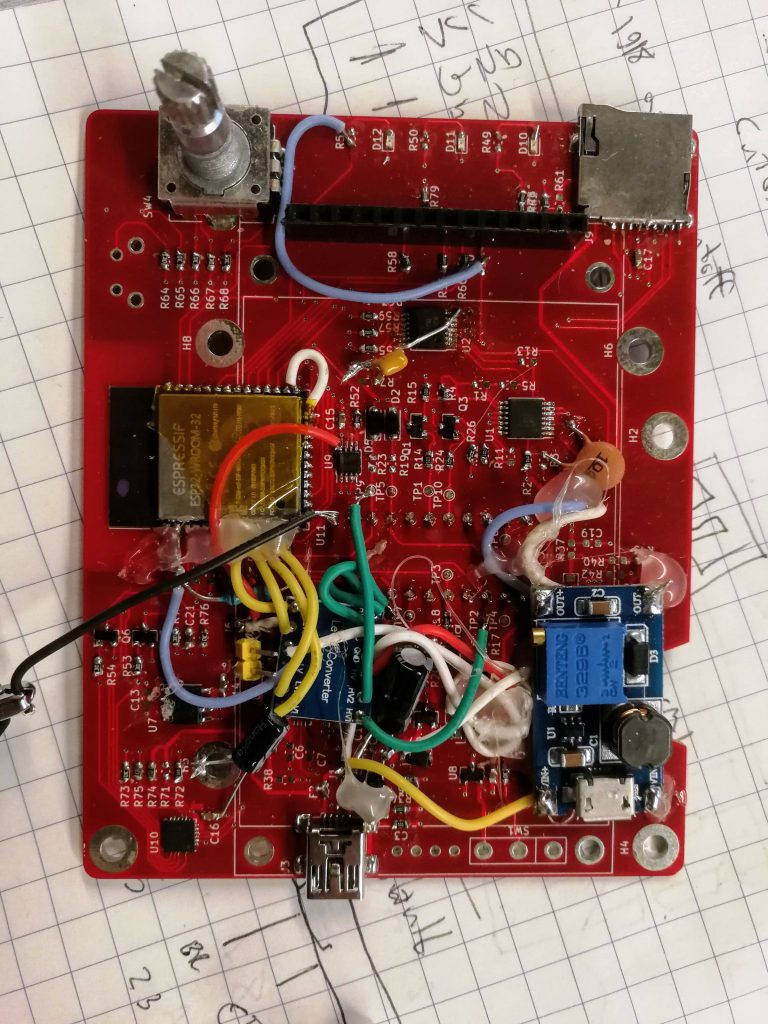
Obviously lots of bodges had to be made. Mostly because of the many voltage rails – the sensor has 5V signaling, while the CCD itself is charged with 12V, the microcontroller is 3.3V, and there’s the whole 5V / battery voltage mess. So this board is more bodge wires and hot glue than PCB at this point.

So how well does it work?

Well, here’s another difference between the original module I used and this sensor: The sensor doesn’t have an integrated lens.

Due to ubiquity, I picked up an M42 camera lens mount for a couple bucks and found a $20 lens on Craigslist. The M42 lens is an old 35mm standard, which is coincidentally just the size of my sensor. Used to be very popular too, so good deals can be had.

However, I have not yet designed a chassis, so anything the image captures will be a blurry mess.

One more issue is that I’m still tweaking the hardware around the analog output. The sensor datasheet recommends feeding its output through the base of a BJT transistor as a sort of transimpedance amplifier. It’s kind of a strange way of doing that, so I’m playing around with proper op amp methods to do that consistently and repeatably. That requires a fair amount more tweaking though, as the datasheet has no information on the nature of the output that is expected. That’s just a matter of putting more time into the investigation, but in the meantime, I have poor dynamic range.

So here’s the first test image that came out of it:


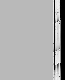
The scan is the red channel only, from left to right. Starting with something dark covering the sensor, and at a very obvious point in time, I removed it and put an object centre of the sensor. I would consider that a success, albeit not as pretty as I’d hoped.

Here’s the object:

In addition to the many above changes, some software updates I’ll write down the line are to integrate better the two obvious viewing modes: waterfall, and histogram. The histogram mode is useful for getting focus right, and then switching over to waterfall mode (as shown above) to see images.

Histograms, similar to the feature that is often available in DSLRs, could show the sensor input intensity as a vertical line on a graph, with pixel position on the horizontal. The steeper the histogram, the sharper the focus.

Syringe Full of Lead

I’ve used a lot of solder paste, usually from one of those big syringes.

When depositing little tiny blobs of solder on a few hundred little tiny pads, two problems emerge:

  1. That big syringe has a big plunger that really starts to hurt the heel of your hand after a lot of usage, especially when the paste is still a little cold from storage. And,
  2. when it’s so challenging, accuracy of deposition goes down.

Yes, both of these problems sound really minor, but they’re actual problems! And solvable!

There are a few different strategies for paste deposition. One of them, which I had a mild infatuation with for a while but never tried personally, uses an air pump connected to a syringe. It drives out the paste with air pressure. Apparently, though, the compression of the air leads to inconsistent and ultimately disappointing results.

Another strategy is to make it electric and attach motor, drivers, and a control system on the back of the syringe. The problem I’ve had with this is that it makes the whole assembly heavy, and therefore difficult to accurately control. The syringe-mounted button also seems like it might cause a little bit of unwanted movement when it’s being pressed.

So, like all quick projects, I let it sit for years while I pondered the issue.

After deciding on a strategy that would allow me to put the least amount of effort into this as humanly possible, I bought the following:

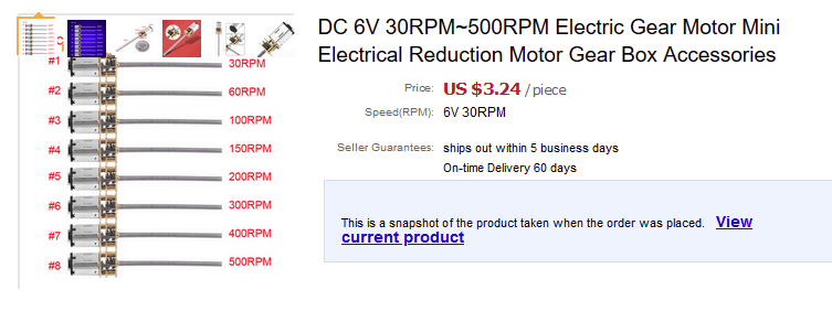
DC motor with gearbox and threaded rod:


Brass heat-set inserts:


1mL syringes:


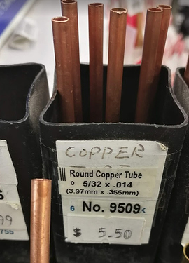
Copper tubing:

And a pile of electronics I already had kicking around.

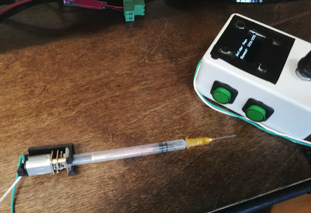
I 3D printed a syringe-motor adapter.

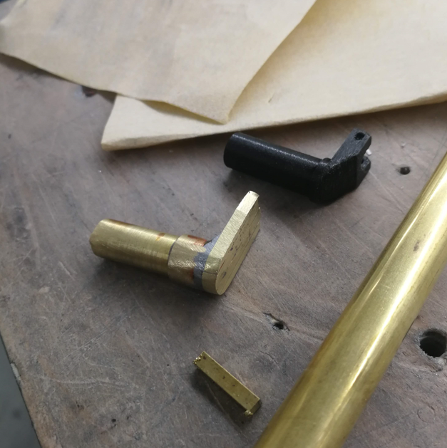
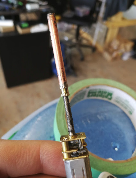
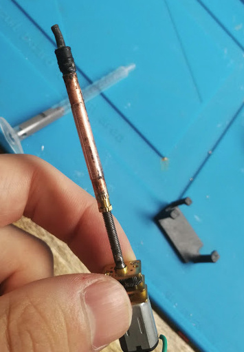
I soldered an insert onto the brass tube, and then with the motor, I had a linear actuator.


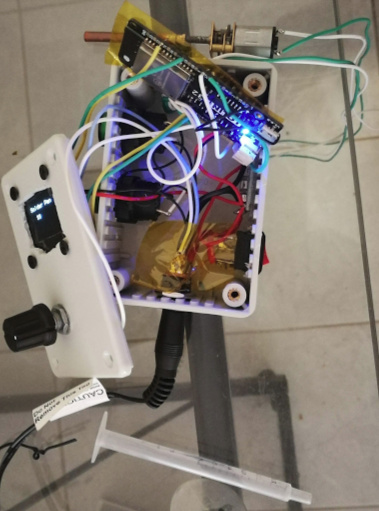
Pile of electronics:


Neat.


I also glued the rubber gasket/tip to the copper tube.


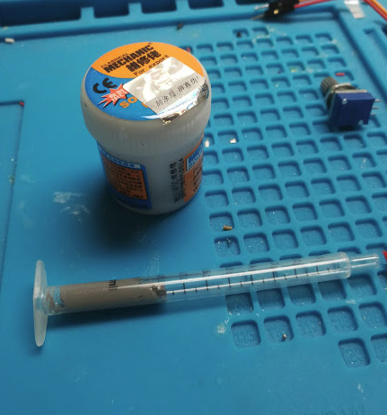
The solder paste I had available is a couple years old, and really chunky/nasty. Solder paste has a shelf life, and paying attention to that is important.


Put it all together anyway:

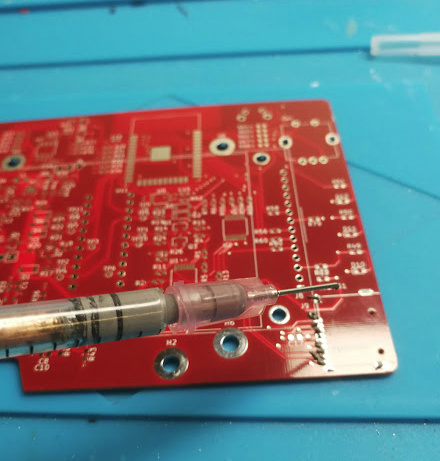
Little bit dribbly at first:


But not bad for a first test:


Obviously not perfect, though. The mechanism stopped being able to force the crusty paste through the needle, and broke the (admittedly flimsy) 3D printed bracket when the motor tried to exit its situation.

Using the flimsy bracket as a mechanical fuse might not even be a bad idea to keep around for future versions. The real problem was the paste, it was toast.

This will definitely be tweaked a lot. I’ll add pullback to the software to prevent the nozzle dripping, and maybe some other features. But it’s a start!

Summertime, and the livin’ is easy

People often ask me, “Jarrett, what is the Best Thing in Life?”

I’m not sure why people keep asking me this, but depending on my mood, the answer is one of two things: Floating on a lake, or swinging in a hammock. At peace with the world.

Frustrated by this bounty of choice that I just couldn’t narrow down, I began righting this wrong in the world.


So I bought a boat.


And I bought a hammock.


And I bolted them together.


It even got me a sweet discount on the boat.


In truth, it actually took several false starts to build this successfully. Part of the challenge was that I wanted to avoid making any permanent modifications to either of the two structures, and the other difficulty is that while mulling over the challenges, well, I had a hammock in which to ponder design decisions. It’s nigh impossible to exit a hammock once you’ve settled in: fact.

The hammock frame is made out out of steel tubing, but the pontoon boat’s frame is aluminum. This made things a little challenging. No welding, really.


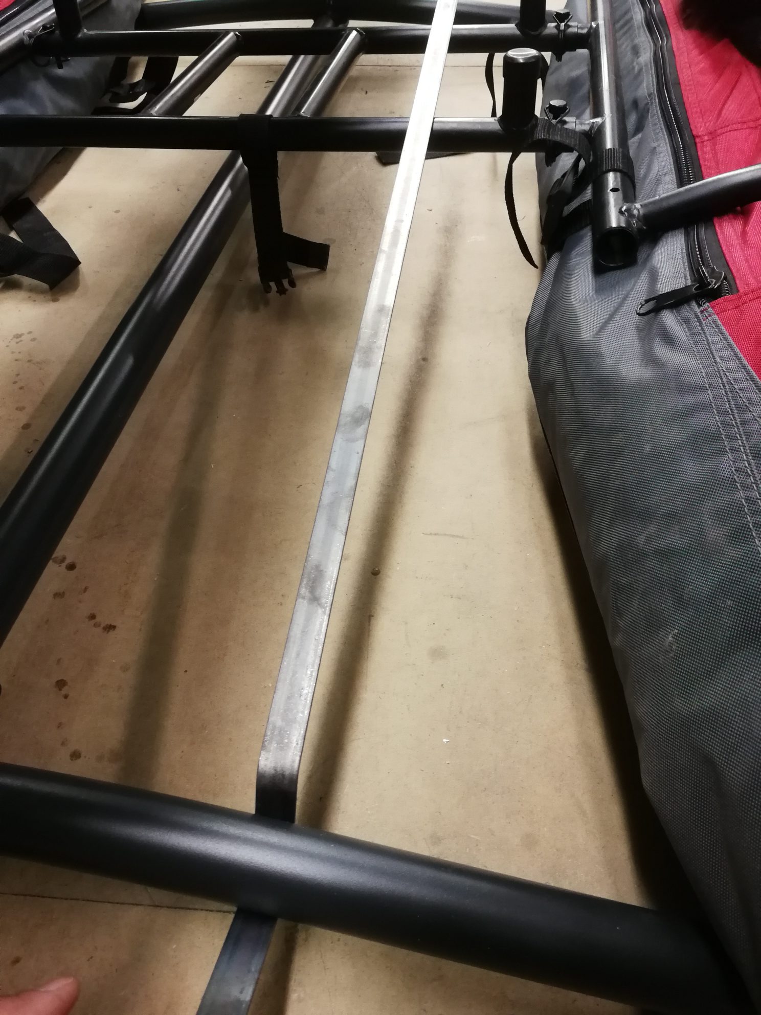
My first attempt used some steel flat stock.

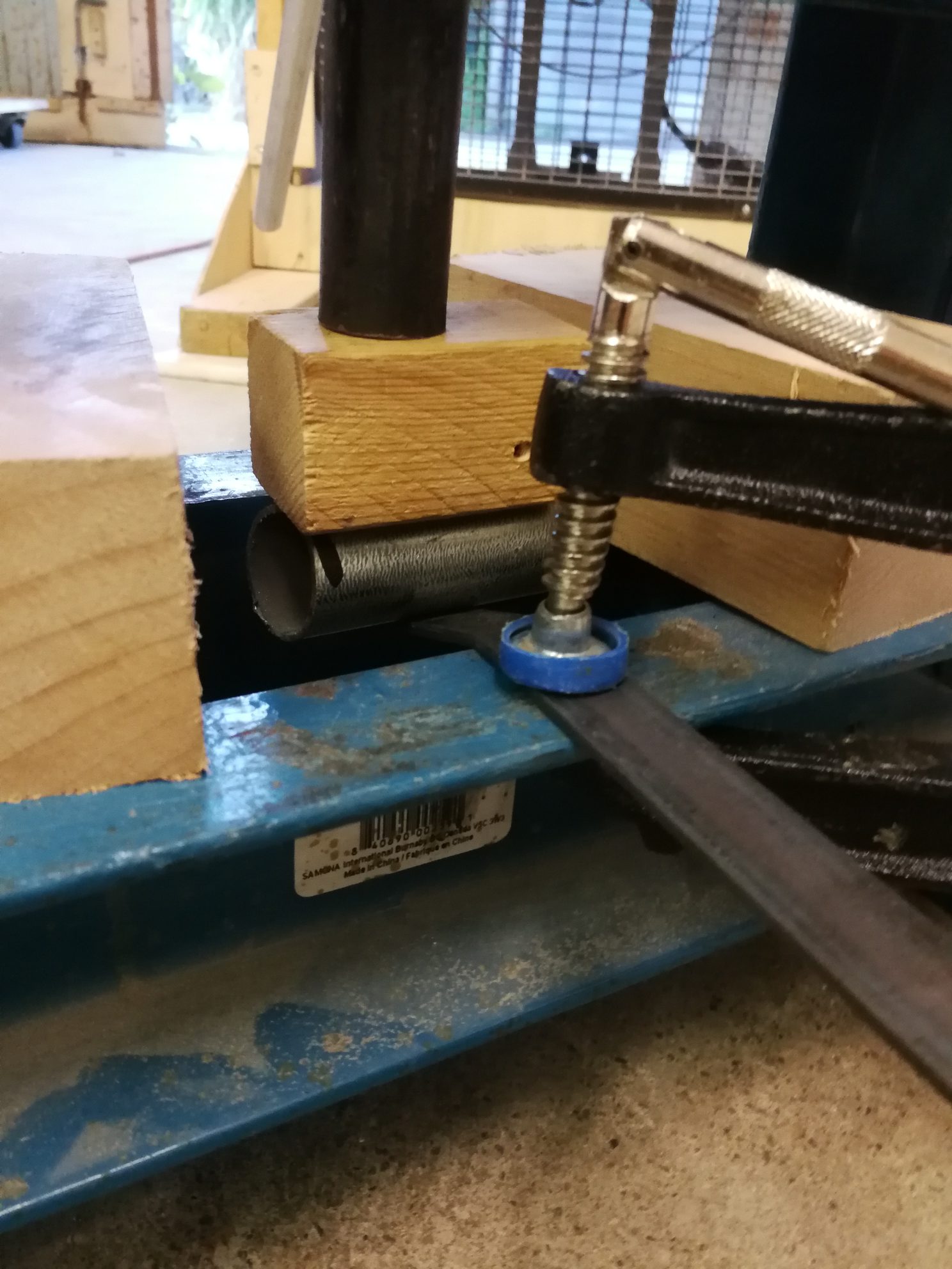
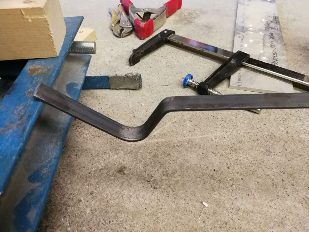
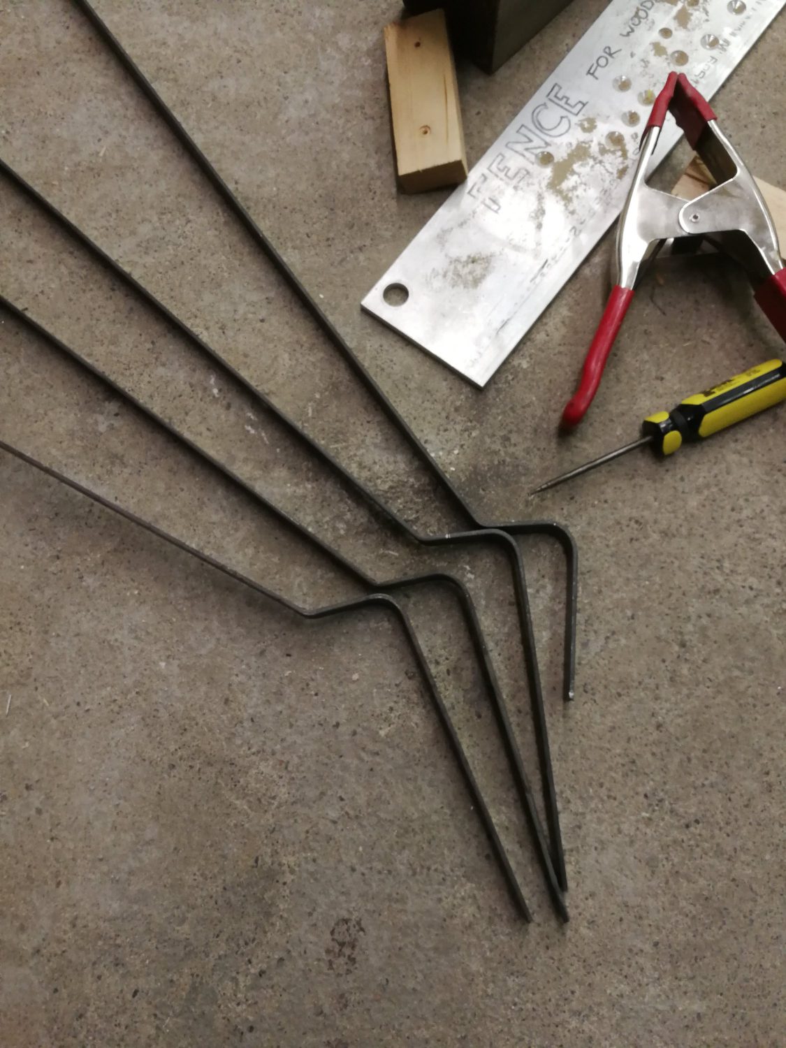
I used a hydraulic press in an only sort-of-sketchy set-up to bend them in a half circle to go around the hammock frame’s steel tubing.


While putting any kind of weight on these, they’d bend distressingly, and have a sort of spring effect that I could see multiplying forces in weird ways, so I decided to abandon that route.

That made me sad, though, look at those bends!


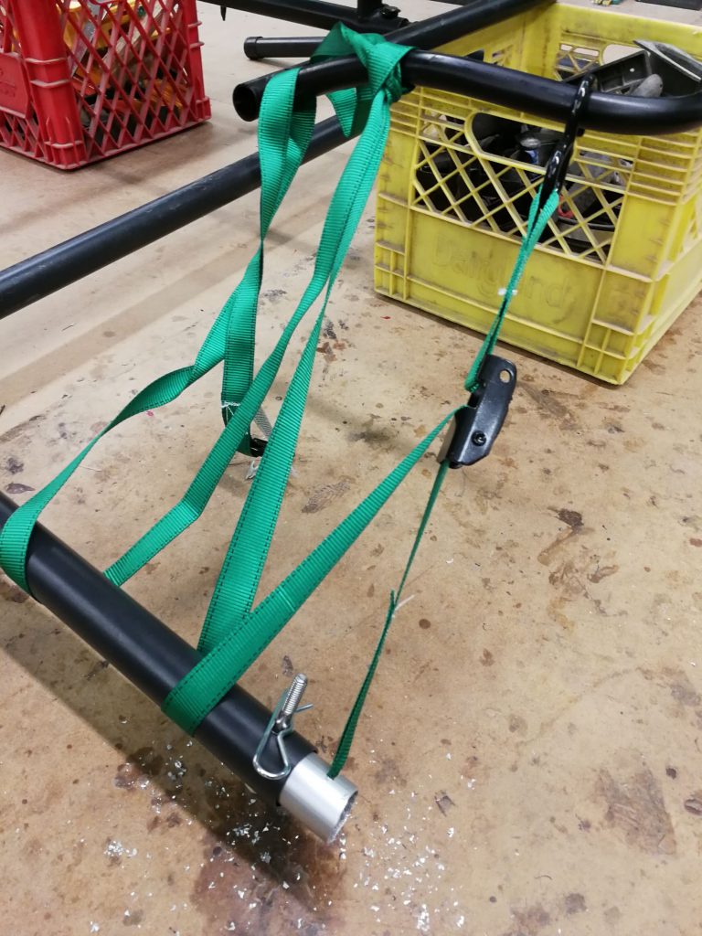
In parallel with the above, I also picked up some straps and built a method to fasten them around the pontoons.
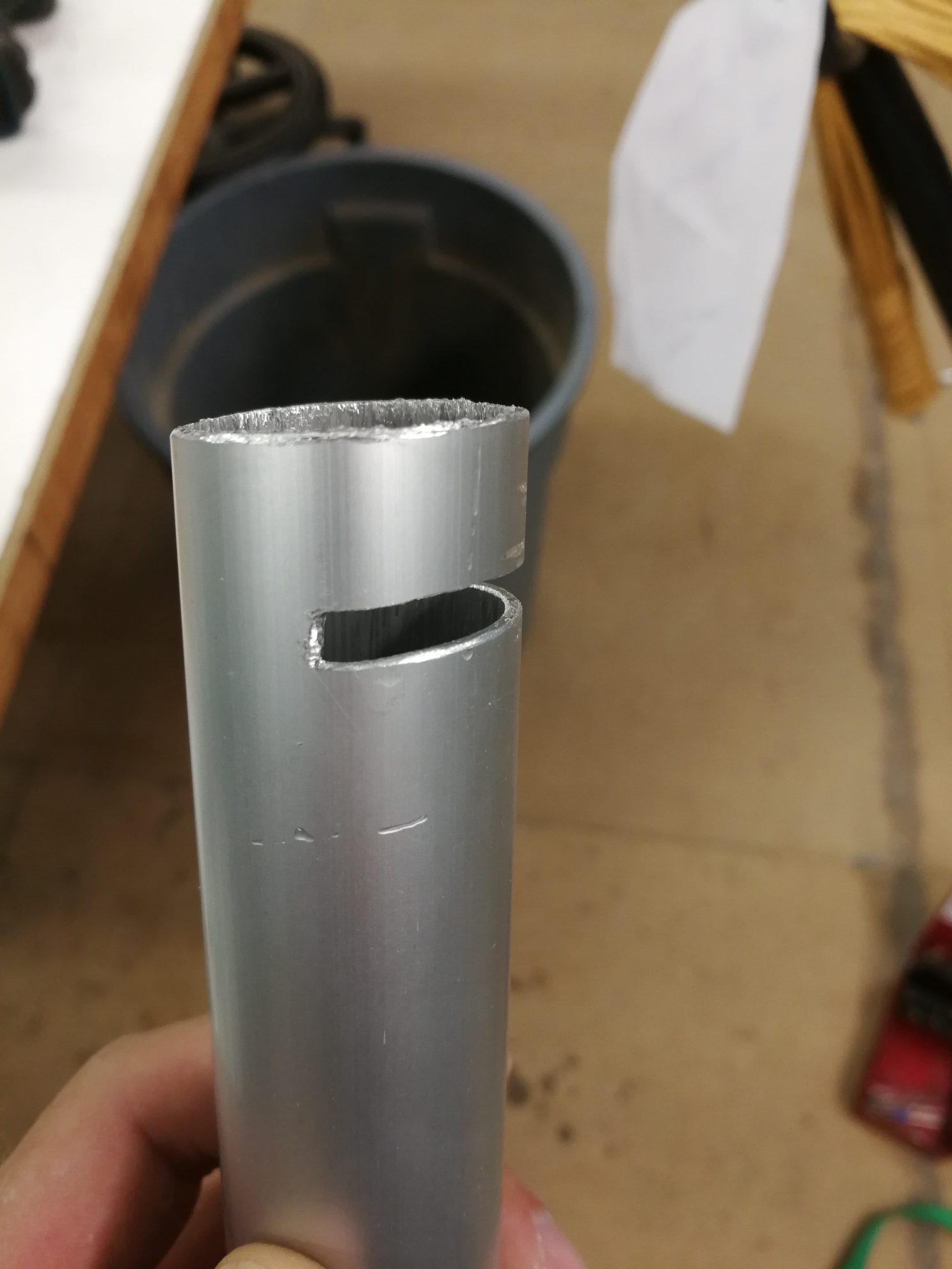
Aluminum tube, a slit, and some filing (oh so much filing) did the trick, along with some new holes, bolts, and cotter pins.


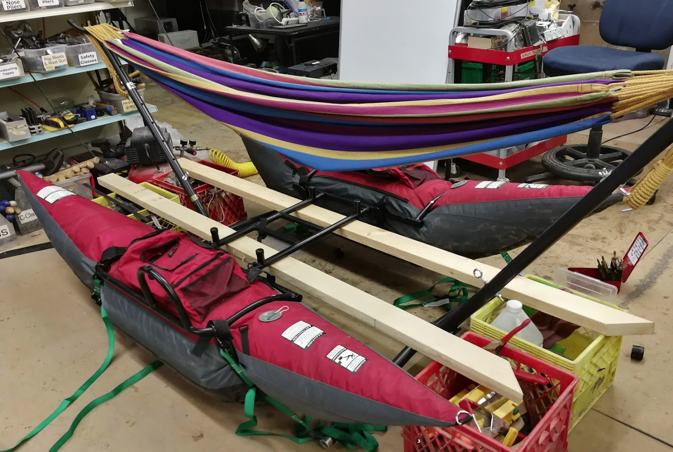
Also positioning the whole contraption without mashing the pontoons against potentially sharp machine shop floor was tough. I finally settled on this lumber solution, which helped me see the final fastening solution.


Back to the scrap bins, I found nearly the identical black anodized aluminum tubes that the pontoon boat is made out of. They slot right into the existing frame and couldn’t be more perfect. I hear they’re from an old bedframe.

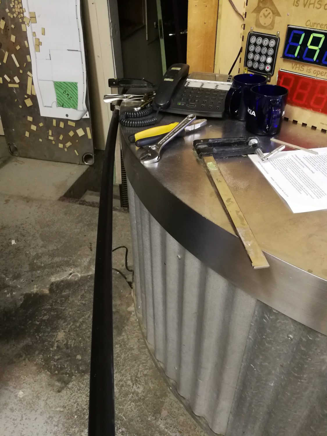
First I tried to bend one.


Then I tried harder to bend it.


Naturally, I kinked it, but I continued to try to bend it, this time using a convenient streetlamp garden decoration.


I still couldn’t get the bend angles I needed! Just not strong enough or heavy enough or clampy enough! I abandoned that attempt.

So attempt number, whatever.

I tossed two more of those scrap tubes into the boat frame, and clamped it on with some u-bolts.


Well that was easy. It brought the hammock a liitttle higher than I really wanted, but I decided to gopher it and fix it in rev 2 if it was a disaster. Summer is running out.


Before launch day, with much thought and much more relaxing hammock meditation, I decided that the boat tooootally had enough side-to-side stability, and that I’d have more issues front-to-back. This is because the hammock in resting position really wasn’t too much higher than the original boat’s seat, but the leverage on the hammock’s front/aft mounting points was way further out than the pontoons.
This later turned out to be completely correct.

But, burn that bridge when we get to it! I will probably add an outrigger to the back of the hammock frame. The water wings and pool noodles are not intended to be used, they’re just there as a last resort hammock rescue device, which we didn’t need.

And grab a couples friends and off we go.


Here’s the maiden voyage:


Spoiler:


But with a little more careful weight distribution, it works! It actually works really well, I was kinda blown away. It’s pretty much the best thing ever and I can’t believe it didn’t kill me.

Bliss.

POV Globe – The Mechanicals

The mechanical design for this project follows the “as quickly and easily as possible” maxim even more so than any other section. I used flat pack laser cut design strategies that results in pieces that snap together. I like that because it could in the future be turned into a kit reasonably easily, and in the meantime, it’s just a quick way to design and iterate.

For this first version, aesthetics plays no part, I just wanted to get the PCB mounted and spinning, along with an appropriate motor.

I used off the shelf mechanical components wherever possible, too. Standard bearings, shafts, collars, and couplers. Oh my.

Coupling the PCB to the drive shaft was a challenge that went through a few ideas to keep it manageable. Something off the shelf, or quick and cheap to manufacture. 3D printing is right out. This picture illustrates the problem, along with a laser cut mock up of the PCB:

One of the solutions I explored was to use clevis pins, intended for RC helicopters.

I found some aluminum ones and some nylon ones, but the former ended up being unsuitable for size. The nylon still wasn’t perfect, but here’s a tip for when your shaft is inappropriately large:

You can grind down steel rods to make a serviceable cutting edge, turning it into a poor-but-functional drill bit. Then they’ll drill right into the nylon.

One more issue was battery holding. Ideally, I wanted a cylindrical battery (or batteries) held longitudinally in the centre of the sphere. That seemed best for keeping the spinning disk balanced. For electrical reasons, I chose three LR44 coin cells stacked up to make 4.5v nominally.

After much fruitless battery holder searching, I grabbed a 12mm ID acrylic tube, and cut away part of it such that it could be fit into the PCB and then twisted to lock it in place. Like so:

That actually locked together pretty solidly, and I added a battery spring to the PCB to hold the batteries together.

For the overall frame, I tossed something together in Fusion 360:

With the very first cutting, made from totally scrap laser material – mostly acrylic, but some plywood in there for good measure – I found a minor setback: I had the wrong belt size.

I’m not sure if I calculated wrong the first time, or did some redesigns after purchasing my belt or what, but a second calculation did confirm that my on-paper expectations should have matched my physical fit. I had a 300mm belt, but 82mm between centres at the middle of the adjustment distance, so there was no way that was going to fit.

A 200mm belt proved much more suitable and revealed the next issue, which I vaguely suspected would crop up.

First of all, the system worked. Laser cut pulleys work great, I’ve used them before on other projects, and my tension and belt driven design seemed good.

When that main shaft got split and attached to my PCB mock up, however, the shaft was no longer properly supported.

The belt put leftwards force on the shaft (1), causing it to cantilever in that direction (2), and then cause the pulley to rub against the bearing block (3).

I was hoping that the two bearings above the belt would fully constrain the system, but alas, there is too much flex in the shaft or slop in the cheap bearings, with not enough distance in between them.

So, version two. This time with a supported shaft on either side of the driven pulley. I was trying to avoid that because the design and assembly both get a little more complicated.

One more change was getting rid of the clevis pins. They rattled and I didn’t like them. Instead I swapped the smooth shafts out for D-profiled versions, and laser cut a notched circle to couple with the PCB.

After cutting and reassembly, it works great!

No more mechanical changes need to be made for this prototype to demonstrate that it works. Next section!

LiPo Systems with USB Power

I’ve alluded to this in the past, once or twice.

Power management in battery applications is pretty tricky. There are a lot of different situations, and a lot of different strategies. In the past, for the topic of this conversation, single cell Lithium polymer batteries, I’ve used a pair of Schottky diodes to automatically “select” the highest voltage feeding the system. That will be either 5V USB power, or 3V-4.2V LiPo battery.

It was suggested to me to use the body diode of a P-Channel MOSFET, but I dismissed that as unnecessary: the body diodes have no lower voltage drop than a Schottky, around 0.2V. Here is one of the more readily available results for battery/wall-power switchover:

https://electronics.stackexchange.com/questions/105053/li-po-charging-circuit-question-switching-between-battery-and-power-supply

That thread doesn’t make a good case for the FET solution over the diode, but the initial suggestion to me indicated that, once “on”, MOSFETs will conduct current in either direction. This breaks my understanding of how they work, but it warrants more research.

That search on its own is confirmed by:

https://electronics.stackexchange.com/questions/48646/in-an-nmos-does-current-flow-from-source-to-drain-or-vice-versa

Stack Exchange posts don’t make for good engineering, though. This calls for a simulation!

Initial results check out! Those output waveforms on V(out) and V(out2) should be identical, if the current through M1 was purely through the body diode.

Simplifying this even more, we can do this:

That results in the following waveforms. You can clearly see the shoulder in V(out3) (blue), where the MOSFET transitions from conducting through the body diode, to conducting through the transistor junction itself:

That’s pretty conclusive. It’s weird to find gaps in my understanding of basic electronic building blocks at this point, but I’m always on-board with more education.

So now this is a documented solution at handling the power switching circuitry between USB and lithium batteries.

In the future, I should put together a written record of the strategies for charging the LiPo batteries in the circuit, and also low-voltage cut-offs to avoid over-discharging and permanently damaging the batteries.