As with most of my projects lately, I’m finding that I’m playing catch up with the documentation, so this is an old one.
This project is a bit of a twofer, because it was the demo project for Stretch, my Kicad plugin. Did I say I have a backlog? Stretch was a pandemic project, initially written in March-May of 2020.
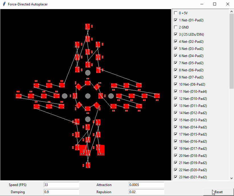
Stretch was the product of me being a little bit frustrated with the state of doing PCB art. Or even just a normal PCB that has some weirdness to it. Something more than the standard utilitarian rectangle with silkscreen labels.
Tools to do art existed, as well as tools to create sophisticated PCBs, but nothing really bridged the gap. The idea is that you can work in Inkscape (or Illustrator, or any other vector tool), which works great for drawing images or curvy lines, but lacks any kind of net information, or DRC, or the limited pallet of a PCB tool.
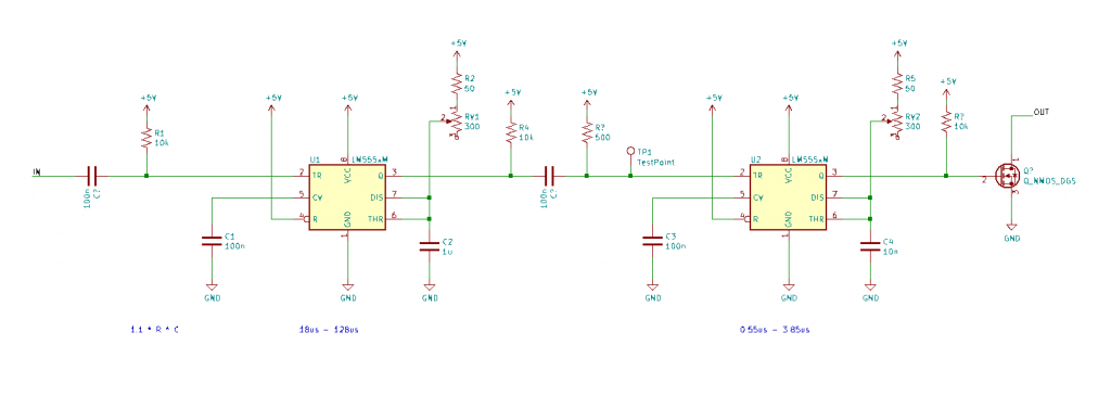
So the workflow is like this:
Users can start by drawing a schematic and laying out a PCB, then bring it into Inkscape to arrange a thousand LEDs into a flower arrangement, then bring it back into KiCad to lay out traces, back into Inkscape to curve the traces, back into KiCad to change their microcontroller and few pin assignments, back into Inkscape to draw out some silkscreen patterns, back into KiCad to run DRC, and so on. The workflow is intended to be seamless and painless to go back and forth.
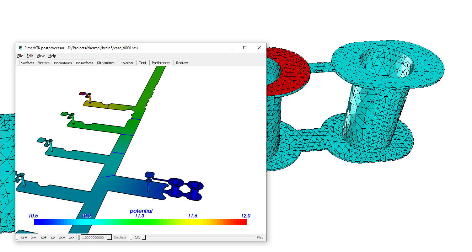
See the repo here. It still, as of this writing, mostly works, but it will likely choke up on certain fields in the file format and need fixing. Regrettably, after tracking KiCad file format changes for three versions, I’ve had to abandon work on this. It’s a constant moving target that is poorly documented because, to be fair to the KiCad dev team, this is way off-script for how you’re supposed to build KiCad extensions.
If I were to do this more recently, there are now a few projects that parse the KiCad file structure that I could piggyback off of. But at the time, I was one of the first people doing a bunch of “parse an evolving undocumented format” work myself, which is exactly as fun as it sounds.
Even more recently, KiCad 9 has a new (still somewhat work-in-progress) scripting system that seems promising. I have plans for future projects, as soon as certain features get implemented.
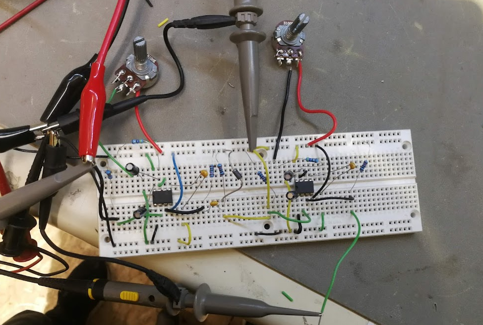
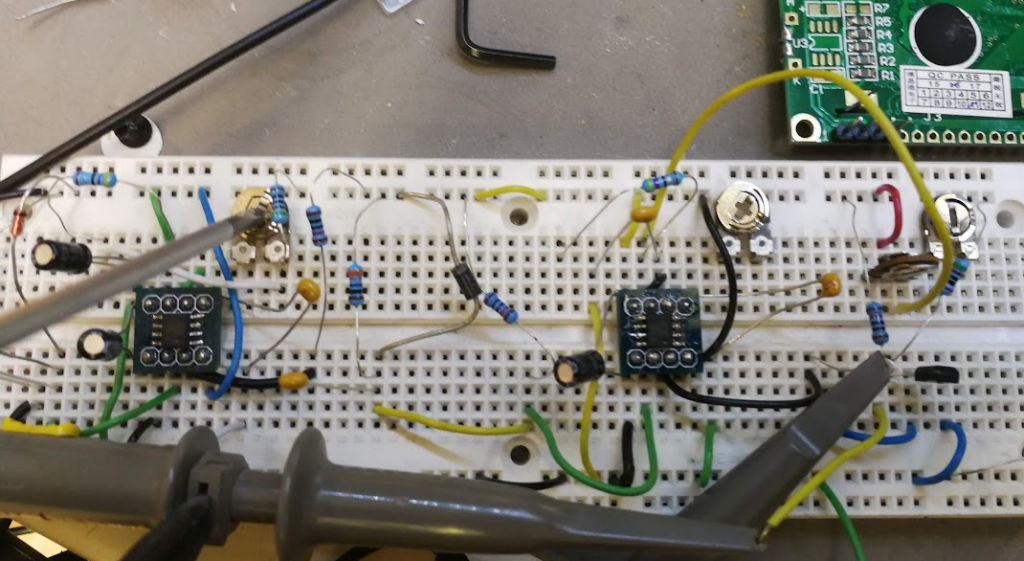
So now we get to the project that I built alongside Stretch. I really wanted to polish this off before posting about it, but I have to get it off my plate.
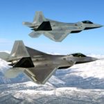
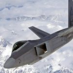
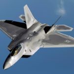
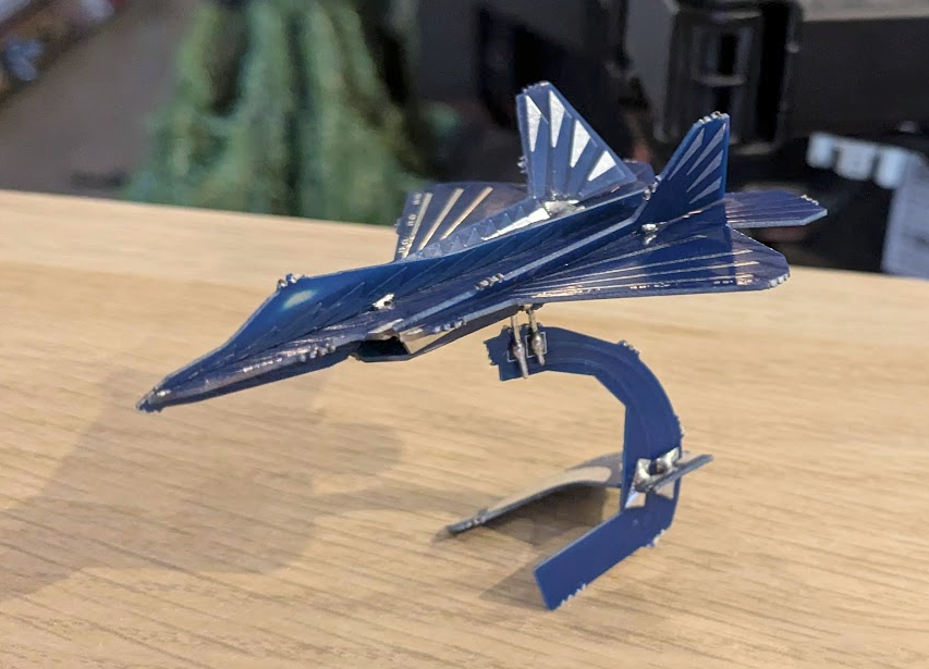
The F-22 is one of the two best looking fighter jets in existence, along with the MiG-29. I wanted to build something out of PCB material, with traces crossing the boundaries of different PCB sections.
The F-22 lends itself well to this:
-
- (U.S. Air Force photo)
-
- (U.S. Air Force photo by Senior Airman Laura Turner)
-
- (U.S. Air Force photo/Master Sgt. Andy Dunaway)
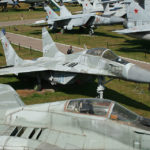
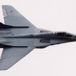
The MiG-29 has a lot of flowing lines that don’t:
-
- (AVIA BavARia)
-
- (Jo Mitchell)
Alongside that, I really like flatpack model kits.
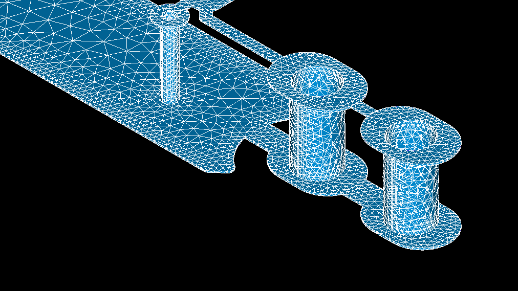
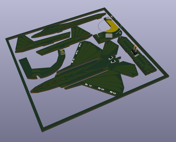
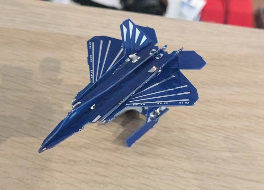
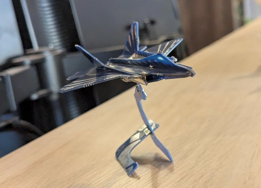
So I built my own, out of FR4 PCBs. The idea with also using an ECAD package was that I could route traces through the object, in 3D, and wind up with circuitry in cool areas.
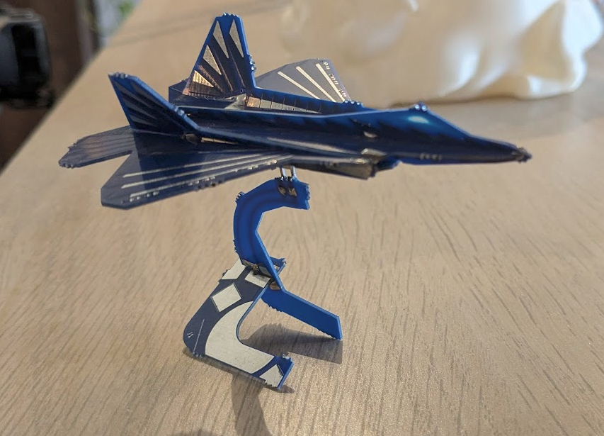
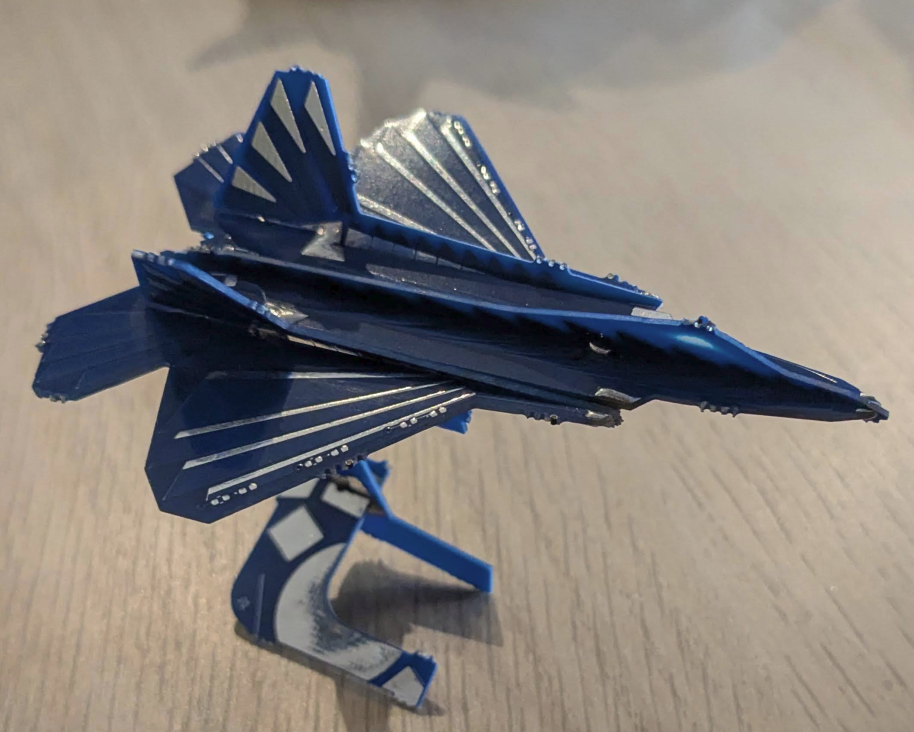
The obvious first thing I did was put LEDs on the wingtips, fed from a battery in the base (which can also act as ballast). Initially I wanted to also add some pulsing circuitry, right on the wings, but this project also blew up a little in terms of time/work, so I kept it simple and just added PCB art. In the same plane-type vein, it would be totally possible to add a (spinning, but not useful) propeller to the front of a biplane, using PCB motors.
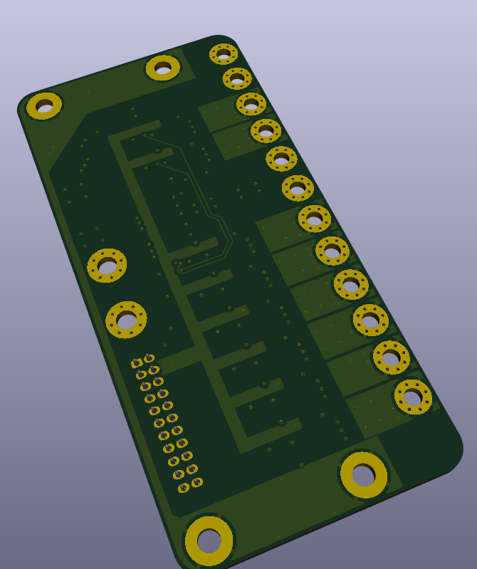
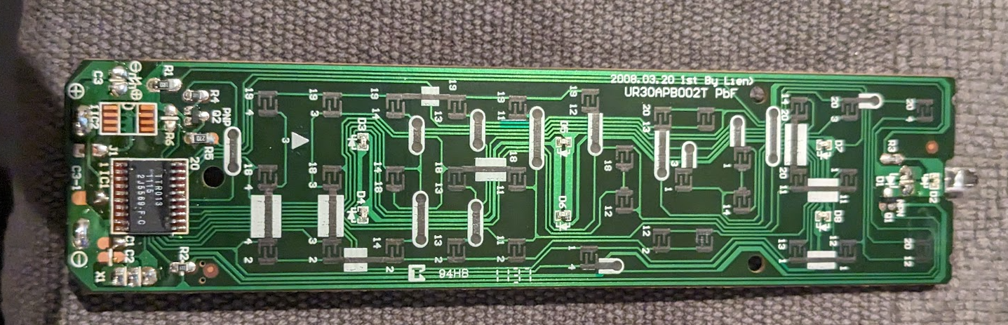
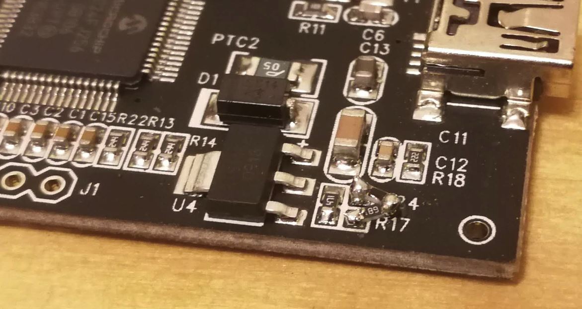
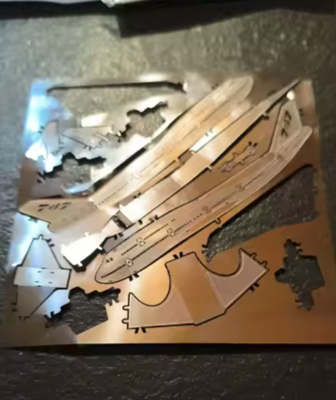
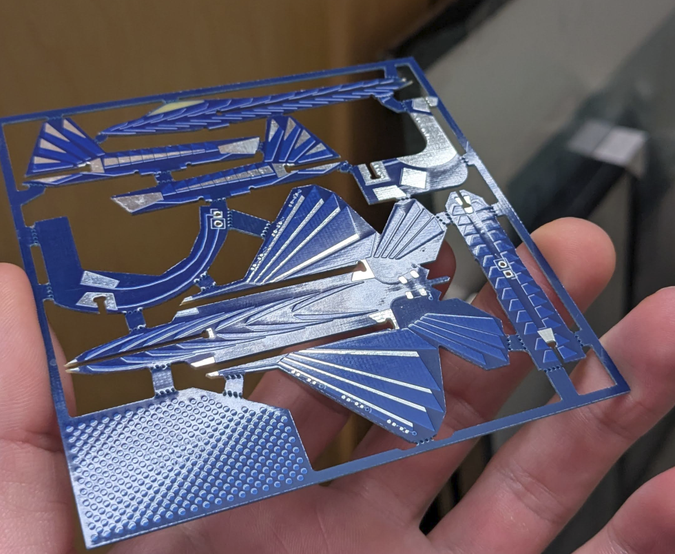
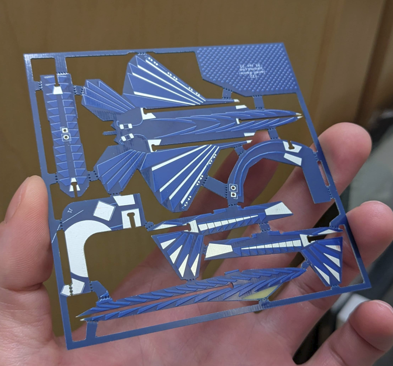
Obviously this particular model shown doesn’t have any of the components soldered, or the mousebites filed down.
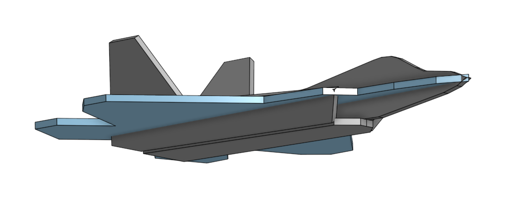
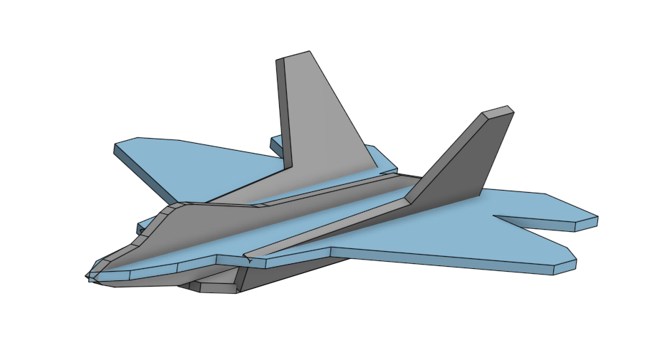
I started by modelling the pieces and fitting them up in OnShape.
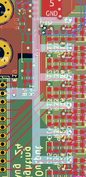
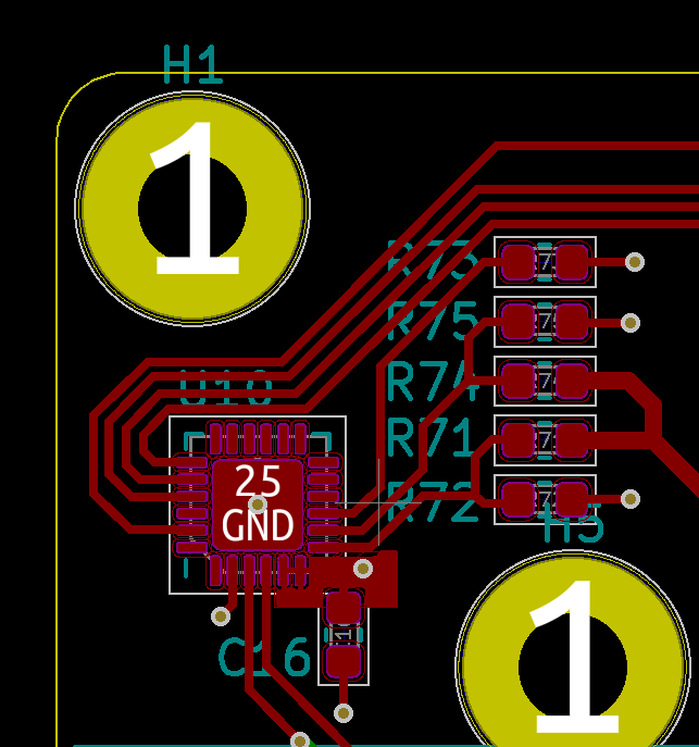
Then a simple LED and battery schematic was drawn in KiCad, transferred to a PCB, and then using Stretch, brought over to Inkscape, where the outline of each piece was added, exported from OnShape. And then back and forth between KiCad and Inkscape for a bit, drawing nice details, or making sure the LED nets go properly through each of the soldered joints.
 (Shown here before mousebites added)
Anyway, it worked! It looks pretty nice. Combining all of the difficulty of designing a flatpack sculpture with all of the difficulty of a nice / functional piece of functional art, while also writing the tooling to make it less painful turned out to be a lot of work. And then building it at the end, too! It tested my patience.
This first version was missing a couple copper pours in the corners with which to solder the joints together.
The first version was manufactured by PCBWay, which is coincidental because I have another project coming up that they helped me with. So they’re not even incentivizing to talk about how great they are, with this one. After sending this in for review, they asked me if they could change some stuff to improve yield, which I reviewed, and even got them to send back their suggested changes on the gerber file.
Fun manufacturing details: Copper etchant likes a roughly even amount of copper on the whole surface. So if you have a PCB that has almost no copper on one half of a layer (ie. everything etched away), and almost entirely copper on the other half of the layer (nothing etched), then the etching process won’t have a happy medium and cause either over- or under-etching in some areas of the board.
PCBWay looked at my files, figured this would be an issue, and here’s the cool part: determined that the corner of my board wasn’t part of the art piece, and filled only that area up with the copper polka dots you see there. Anyway, I was impressed.
For revision 2, I went with a different boardhouse (slightly cheaper) and the quality was actually a bit unacceptable, if I wanted to produce these for anything other than this one-off project. Here’s the R2 model – Check out the terrible soldermask bleed in the cockpit area, and there are some other cosmetic issues.
Getting the electronics working, or maybe doing something cooler with them, and cleaning up some areas (like mousebites in less obtrusive areas) may be a future project when I pick this up again. Something that could be cool as a model kit.